Display device and method for measuring surface structure thereof

A technology for a display device and a measuring device, which is applied in the fields of display device and measurement of its surface structure, display device surface structure and measurement of its surface structure size, can solve the problem of inability to obtain uniform reflected light, decrease in product yield, and measurement of structure size Problems such as poor accuracy and reproducibility of results

Inactive Publication Date: 2010-12-01
华映视讯(吴江)有限公司 +1
View PDF0 Cites 1 Cited by
  • Summary
  • Abstract
  • Description
  • Claims
  • Application Information

AI Technical Summary

Problems solved by technology

[0004] However, in order to arrange more pixels in a smaller space to provide higher resolution, the width of the light-shielding layer between each pixel must be reduced and cannot provide a single plane with sufficient width, so that the measurement beam is irradiated on the patterned surface. When the light-shielding layer 214 cannot obtain uniform reflected light, the accuracy and reproducibility of the measurement results of the structure are not good, which in turn causes difficulties for the manufacturing engineering that relies on the measurement results to adjust the manufacturing parameters, resulting in a decline in product yield and The downside of reduced yield

Method used


Image

  • Display device and method for measuring surface structure thereof
  • Display device and method for measuring surface structure thereof
  • Display device and method for measuring surface structure thereof

Examples


Embodiment 1

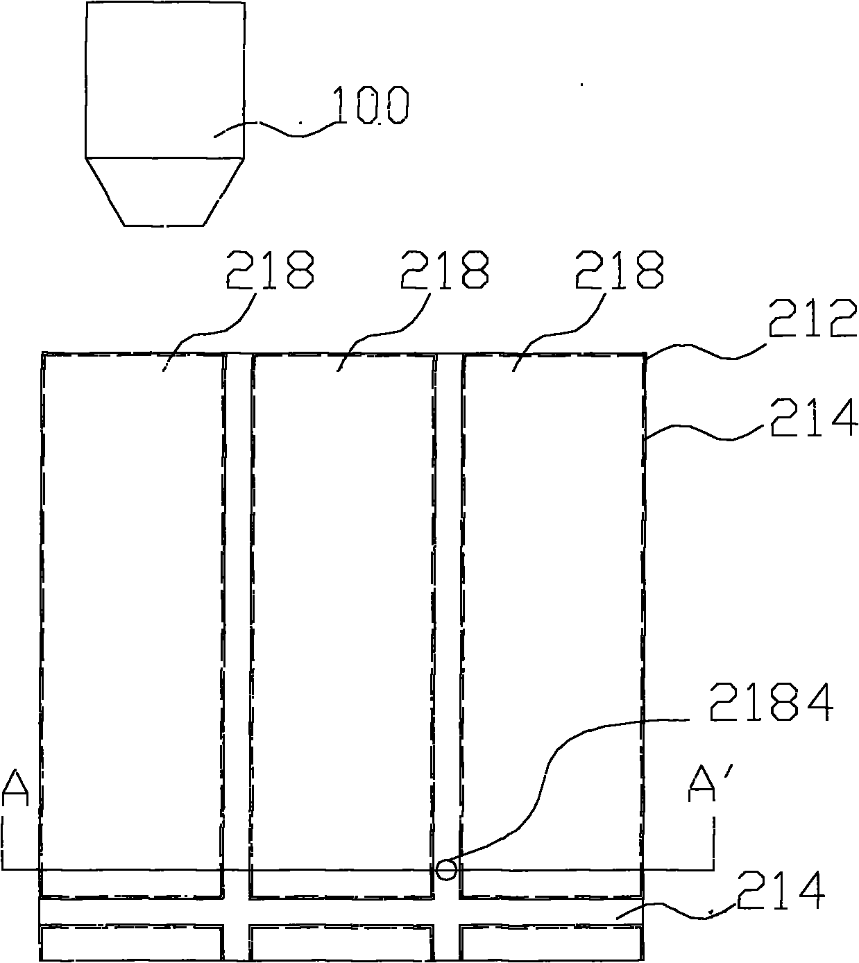
[0021] see Figure 5 , a display device 300 according to an embodiment of the present invention, such as a liquid crystal display, includes: a first substrate 310 having a first surface 312;

[0022] a first patterned light-shielding layer 322, including a plurality of first openings 324, disposed on the first surface 312 of the first substrate 310;

[0023] at least one second patterned light-shielding layer 332, including a plurality of second openings 334, disposed between the first patterned light-shielding layers 322 on the first surface 312 of the first substrate 310;

[0024] At least one first pixel unit 326 includes:

[0025]At least one first red filter layer 326R, at least one first blue filter layer 326B, and at least one first green filter layer 326G cover the first openings 324 of the first patterned light-shielding layer 322 respectively. and a part of the first patterned light-shielding layer 322;

[0026] At least one columnar spacer 328 is disposed in the ...

Embodiment 2

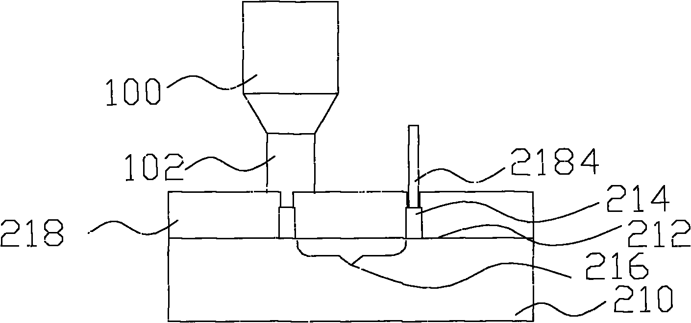
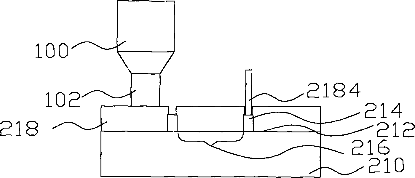
[0033] see Figure 5 and Figure 6 , Figure 6 for Figure 5 The plan view of the first substrate 310 of the present invention, the method for measuring the surface structure of the display device according to the second embodiment of the present invention includes:

[0034] A display device 300 is provided, such as a liquid crystal display, comprising: a first substrate 310 having a first surface 312;

[0035] a first patterned light shielding 322, including a plurality of first openings 324, disposed on the first surface 312 of the first substrate 310;

[0036] at least one second patterned light-shielding layer 332, including a plurality of second openings 334, disposed between the first patterned light-shielding layers 322 on the first surface 312 of the first substrate 310;

[0037] At least one first pixel unit 326 includes:

[0038] At least one first red filter layer 326R, at least one first blue filter layer 326B, and at least one first green filter layer 326G co...


PUM


Abstract

The invention discloses a display device and a method for measuring a surface structure thereof. The display device comprises a first base plate, at least one first imaging shading layer, at least one second imaging shading layer, at least one first pixel unit, at least one second bump, and at least one second pixel unit, wherein the fist base plate is provided with a first surface; the at least one first imaging shading layer comprises a plurality of first opening parts; the second imaging shading layer comprises a plurality of second opening parts and is arranged between the first imaging shading layers on the first surface of the first base plate; the first pixel unit comprises at least one bump which is covered on the plurality of opening parts of the first imaging shading layer; the at least one second bump is arranged in the first imaging shading layer and the plurality of the second imaging shading layer; the at least one second pixel unit comprises the at least one third bump; and the size of the second opening parts of the second imaging shading layer is smaller than that of the first opening parts of the first imaging shading layer. A reflection plane provided by the second imaging shading layer is larger than that provided by the first imaging shading layer, so the measurement result of the clear height of the second shading layer is more precise and reproducible than that of the first shading layer.

Description

technical field [0001] The present invention relates to a display device and a method for measuring its surface structure, in particular to a display device surface structure and a method for measuring its surface structure size, which are applied in the field of display devices. Background technique [0002] In recent years, display products have been designed with the concept of light, thin, short, small, and high resolution, but such requirements have made the design, manufacture and size measurement of the internal structure of the display very difficult. Setting more pixels in the space to provide higher resolution often results in insufficient space between various structures, resulting in poor accuracy and reproducibility of the results of the size measurement of the structures, which in turn makes it difficult to rely on the size measurement results to adjust the manufacturing The manufacturing engineering of parameters causes difficulties, resulting in the disadvant...

Claims


Application Information

Patent Timeline
Patent Type & Authority Applications(China)
IPC IPC(8): G02F1/1335G02F1/167G01B21/02
Inventor 林志维王闵正陈雍程刘泓旻
Owner 华映视讯(吴江)有限公司
Why Eureka
Try Eureka