Semiconductor packaging member
A semiconductor and packaging technology, applied in the field of semiconductor packaging, can solve the problem that the bonding degree between the flip chip 14 and the substrate cannot be further improved
- Summary
- Abstract
- Description
- Claims
- Application Information
AI Technical Summary
Problems solved by technology
Method used
Image

Examples
Embodiment Construction
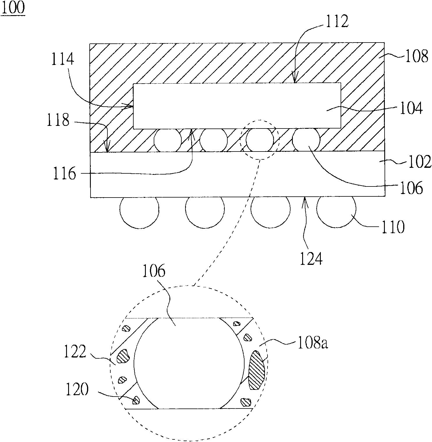
[0030] Please refer to figure 2 , which shows a cross-sectional view of a semiconductor package according to a preferred embodiment of the present invention. The semiconductor package 100 is, for example, a Flip Chip CSP. The semiconductor package 100 includes a substrate 102 , a semiconductor component 104 , a plurality of component contacts 106 , an encapsulant 108 and a plurality of substrate contacts 110 .
[0031] The substrate 102 has a first surface 118 and a second surface 124 opposite to each other. The semiconductor device 104 is, for example, a flip chip disposed on the first surface 118 . The substrate contacts 110 are, for example, solder balls, conductive pillars or bumps, which are formed on the second surface 124 of the substrate 102 for electrically connecting an external circuit (not shown) and Semiconductor package 100 .
[0032] The device contact 106 is, for example, a solder ball, a bump or a copper pillar, which is disposed between the substrate 102...
PUM
 Abstract
Description
Claims
Application Information
 - R&D Engineer
- R&D Manager
- IP Professional
- Industry Leading Data Capabilities
- Powerful AI technology
- Patent DNA Extraction
Browse by: Latest US Patents, China's latest patents, Technical Efficacy Thesaurus, Application Domain, Technology Topic.
© 2024 PatSnap. All rights reserved.Legal|Privacy policy|Modern Slavery Act Transparency Statement|Sitemap