Test system for improving photoluminescence test effect of semiconductor material

A technology of photoluminescence and testing system, which is applied in the field of semiconductor materials, semiconductor testing and spectroscopy, can solve the problems of low efficiency, limited excitation efficiency, large volume, etc., and achieve the effect of flexible implementation

Active Publication Date: 2012-07-25
SHANGHAI INST OF MICROSYSTEM & INFORMATION TECH CHINESE ACAD OF SCI
View PDF0 Cites 2 Cited by
  • Summary
  • Abstract
  • Description
  • Claims
  • Application Information

AI Technical Summary

Problems solved by technology

For example: the traditional photoluminescence measurement still continues to use the early excitation light sources for near-infrared short-wave end materials, such as He-Ne and Ar in the visible light band. + , YAG, and He-Cd in the ultraviolet band and other types of gas or solid-state lasers. Although these lasers are developed earlier and more mature, they all have problems such as large size, low efficiency, high price, and inconvenient use. With the continuous extension of the luminescent wavelength of the material to the long-wave direction and the emergence of various complex structural materials, the excitation efficiency of these lasers will be greatly limited, thus reducing the test sensitivity of the photoluminescence method, thereby limiting the test and characterization capabilities of this effective method

Method used


Image

  • Test system for improving photoluminescence test effect of semiconductor material
  • Test system for improving photoluminescence test effect of semiconductor material
  • Test system for improving photoluminescence test effect of semiconductor material

Examples


Embodiment Construction

[0016] Below in conjunction with specific embodiment, further illustrate the present invention. It should be understood that these examples are only used to illustrate the present invention and are not intended to limit the scope of the present invention. In addition, it should be understood that after reading the teachings of the present invention, those skilled in the art can make various changes or modifications to the present invention, and these equivalent forms also fall within the scope defined by the appended claims of the present application.

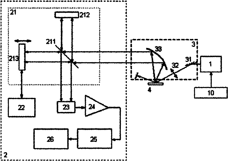
[0017] The embodiment of the present invention relates to a test system for improving the test effect of photoluminescence of semiconductor materials, including a laser, a spectral measurement system and an optical path component. The optical path component includes a reflector, a lens and a parabolic mirror, and constitutes a test optical path; The laser light excited by the above-mentioned laser passes through the mirror and ...


PUM


Abstract

The invention relates to a test system for improving photoluminescence test effect of semiconductor material, which comprises a laser device, a spectral measurement system and light path components, wherein the light path components comprise a reflecting mirror, a lens and a paraboloidal mirror and constitute a test light path. A laser excited from the laser device turns a direction by the reflecting mirror and then directly irradiates the tested sample after being focused by the lens; and the laser reflected by the tested sample is collected by the paraboloidal mirror to turn the direction and be collimated, and then sent to the spectral measurement system in the form of broad beam. The laser device in the invention selects appropriate emission wavelength according to the characteristicsof the semiconductor material, thereby obtaining high photoluminescence strength, enhancing the photoluminescence test capacity and improving the test sensitivity. In addition, the invention does nothave limits and special requirements for the spectral measurement system, and thus, the realization mode is very flexible.

Description

technical field [0001] The invention relates to the technical fields of semiconductor materials, semiconductor testing and spectroscopy, in particular to a testing system for improving the photoluminescence testing effect of semiconductor materials. Background technique [0002] Since the invention of semiconductor lasers in the 1960s, various semiconductor optoelectronic materials have developed rapidly, and their structures have developed from simple bulk materials to complex microstructure materials such as heterojunctions, quantum wells, and superlattices. The scope has expanded from the narrow band in the near-infrared in the early stage to the entire ultraviolet, visible, near-infrared, mid-infrared and even far-infrared bands. The material system also includes VI, III-V, II-VI, IV-VI and organic compounds, etc. And feet. Semiconductor lasers have included distributed feedback, surface emission, and quantum cascade, etc., and their basic structure has also been extend...

Claims


Application Information

Patent Timeline
Patent Type & Authority Patents(China)
IPC IPC(8): G01N21/63
Inventor 张永刚顾溢
Owner SHANGHAI INST OF MICROSYSTEM & INFORMATION TECH CHINESE ACAD OF SCI
Why Eureka
Try Eureka