

CuO-based composite material with high photoelectric property
A technology for composite materials and photoelectric properties, applied in the direction of luminescent materials, molybdenum sulfide, chemical instruments and methods, etc., can solve the problems of limiting photoelectric applications, severe carrier recombination, and many defects, and achieve high light absorption coefficient and temperature window Wide, low-cost effects
- Summary
- Abstract
- Description
- Claims
- Application Information
AI Technical Summary
Problems solved by technology
Method used
Image

Examples
Embodiment 1
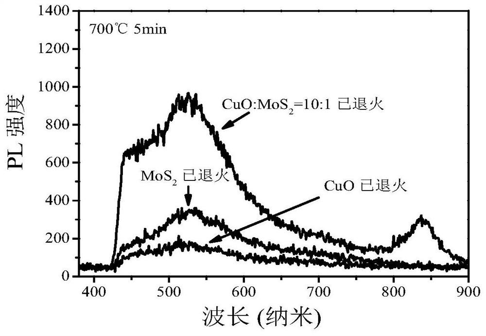
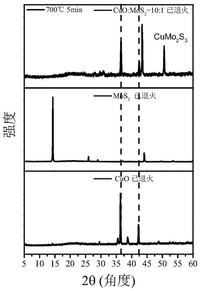
[0023] Combine CuO powder with MoS 2 The powder is fully ground and mixed at a molar ratio of 10:1, and then pressed using a tablet machine at a pressure of 15MPa for 8-10s to form a disc with a thickness of 0.8-1.2mm. The resulting wafer was placed on quartz glass and annealed in an annealing furnace at an annealing temperature of 700°C for 5 minutes to obtain CuO / MoS 2 composite material.
[0024] The material was characterized by photoluminescence (PL) and X-ray diffraction (XRD), the results are shown in figure 1 with figure 2 . figure 1 The PL test results show that the PL peak intensity of the obtained composite material is 4.85 times that of the CuO material obtained under the same annealing temperature and time (the peak value is increased from 200 to 970). figure 2 The XRD test showed that a large amount of CuO and newly formed CuMo were present in the resulting composite 2 S 3 .
Embodiment 2
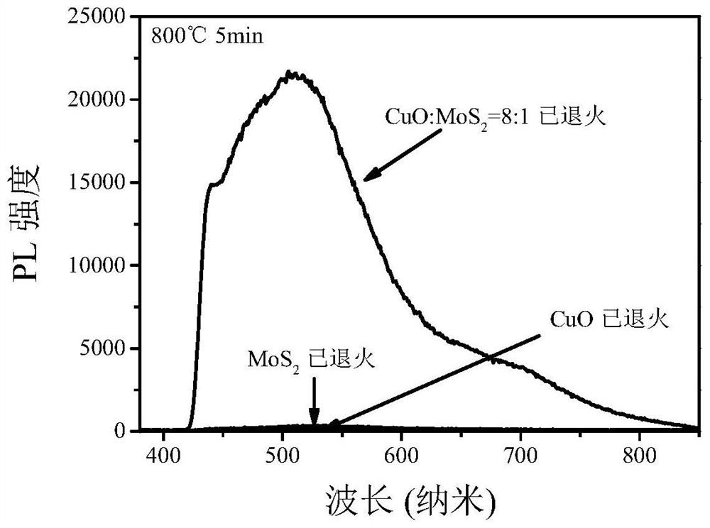
[0026] Combine CuO powder with MoS 2 The powder is fully ground and mixed at a molar ratio of 8:1, and then pressed using a tablet machine at a pressure of 15MPa for 8-10s to form a disc with a thickness of 0.8-1.2mm. The resulting wafer was placed on quartz glass and annealed in an annealing furnace at an annealing temperature of 800°C for 5 minutes to obtain CuO / MoS 2 composite material.
[0027] The material was characterized by photoluminescence (PL) and X-ray diffraction (XRD), the results are shown in image 3 with Figure 4 . image 3 The PL test results show that the PL peak intensity of the obtained composite material is 108.71 times that of the CuO material obtained under the same annealing temperature and time (the peak value is increased from 200 to 21741). Figure 4 The XRD test of the obtained composites shows that there are a large amount of CuO and the newly formed CuMoO 4 .
Embodiment 3
[0029] Combine CuO powder with MoS 2 The powder is fully ground and mixed at a molar ratio of 10:1, and then pressed using a tablet machine at a pressure of 15MPa for 8-10s to form a disc with a thickness of 0.8-1.2mm. The resulting wafer was placed on quartz glass and annealed in an annealing furnace at an annealing temperature of 800°C for 5 minutes to obtain CuO / MoS 2 composite material.
[0030] The material was characterized by photoluminescence (PL) and X-ray diffraction (XRD), the results are shown in Figure 5 with Image 6 . Figure 5 The PL test results show that the PL peak intensity of the obtained composite material is 15.6 times that of the CuO material obtained under the same annealing temperature and time (the peak value is increased from 200 to 3120). Image 6 The XRD test of the obtained composites shows that there are a large amount of CuO and the newly formed CuMoO 4 and Cu 6 Mo 5 o 18 .
PUM
| Property | Measurement | Unit |
|---|---|---|
| thickness | aaaaa | aaaaa |
Abstract
Description
Claims
Application Information