LED epitaxial layer growing method and LED epitaxial layer

A growth method and epitaxial layer technology, applied in the direction of electrical components, circuits, semiconductor devices, etc., can solve the problems of LED device voltage rise, poor anti-static ability, aggravated compensation effect, etc., to reduce the working voltage, good contact, defects low density effect

Inactive Publication Date: 2014-08-20
XIANGNENG HUALEI OPTOELECTRONICS
View PDF5 Cites 22 Cited by
  • Summary
  • Abstract
  • Description
  • Claims
  • Application Information

AI Technical Summary

Problems solved by technology

[0003] Mg-doped: GaN material (P-GaN) has been widely used in GaN-based light-emitting diode (LED) products. In order not to damage the InGaN material of the active layer, the p-type GaN layer is generally grown at a lower temper

Method used


Image

  • LED epitaxial layer growing method and LED epitaxial layer
  • LED epitaxial layer growing method and LED epitaxial layer
  • LED epitaxial layer growing method and LED epitaxial layer

Examples


Embodiment 1

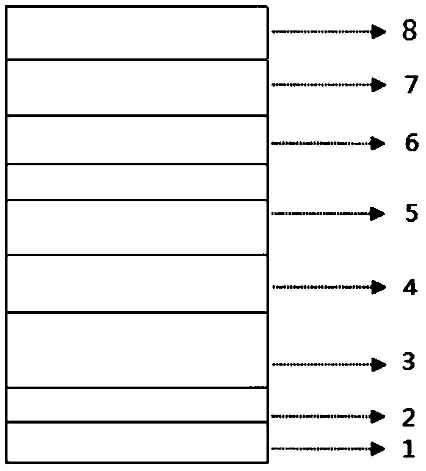
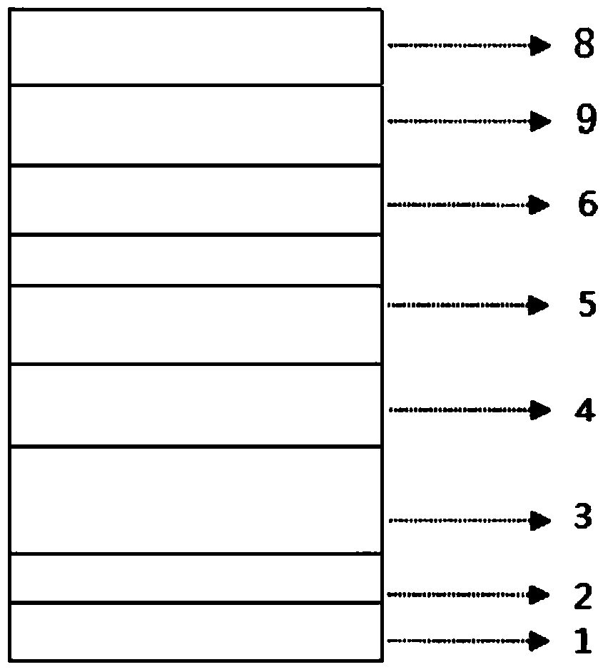
[0046] see figure 2 , the present invention uses AixtronMOCVD to grow high-brightness GaN-based LED epitaxial wafers. Using high-purity H 2 or high purity N 2 or high purity H 2 and high purity N 2 The mixed gas as the carrier gas, high-purity NH 3 As the N source, the metal-organic source trimethylgallium (TMGa), triethylgallium (TEGa) is used as the gallium source, trimethylindium (TMIn) is used as the indium source, and the N-type dopant is silane (SiH 4 ), trimethylaluminum (TMAl) as the aluminum source, and the P-type dopant as magnesium dicene (CP 2 Mg), the substrate is (0001) sapphire, and the reaction pressure is between 100mbar and 800mbar.

[0047] A method for growing an LED epitaxial layer, which sequentially includes processing a substrate, growing a low-temperature buffer GaN layer, growing a non-doped GaN layer, growing a Si-doped GaN layer, growing an active layer MQW, growing a P-type AlInGaN layer, and growing a P-type GaN layer layer step, its opera...


PUM

PropertyMeasurementUnit
Thicknessaaaaaaaaaa
Thicknessaaaaaaaaaa
Thicknessaaaaaaaaaa

Abstract

The invention provides an LED epitaxial layer growing method and an LED epitaxial layer. The method for growing a P-type GaN layer comprises the steps that A, NH3 and Cp2Mg are introduced in a reaction chamber at the temperature of 900 DEG C to 950 DEG C, wherein pressure of a reaction cavity ranges from 200 mbar to 600 mbar, TMGa is closed, and pretreatment of doping Mg is carried out for 10 minutes-20 minutes; B, TMGa is introduced, Cp2Mg is closed, a GaN layer grows for 20 minutes-40 minutes, and the thickness of GaN is 5 nm-10 nm; the step A and the step B are repeated ten to twenty times until the total thickness of the P-type GaN layer is 80 nm-200 nm. According to the method, delta doping is used for growing the P-type GaN layer, the crystal quality of the P-type GaN layer is improved, the dislocation density is reduced, and hole concentration and the migration rate of P-type GaN are improved; more hole-electron pairs can be provided for light-emitting active areas of an LED device, the composite probability is improved, the brightness is promoted, and therefore photoelectric property of the LED device is improved.

Description

technical field [0001] The invention relates to the technical field of LED epitaxial design, in particular to a method for growing a p-type GaN layer by using a delta doping method and an LED epitaxial layer. Background technique [0002] LEDs are widely used in a wide range of fields such as display screens, sensors, communications, and lighting. As the core semiconductor device, GaN-based blue LEDs can be combined with phosphors to produce white light, which is very attractive in terms of lighting. [0003] Mg-doped: GaN material (P-GaN) has been widely used in GaN-based light-emitting diode (LED) products. In order not to damage the InGaN material of the active layer, the p-type GaN layer is generally grown at a lower temperature, resulting in its crystal The quality declines and the compensation effect increases, resulting in an increase in the voltage of the LED device, a decrease in brightness, and a deterioration in the antistatic ability (ESD). Contents of the inv...

Claims


Application Information

Patent Timeline
IPC IPC(8): H01L33/00H01L33/02H01L33/14
CPCH01L33/0066H01L33/0075H01L33/025H01L33/14
Inventor 农明涛
Owner XIANGNENG HUALEI OPTOELECTRONICS
Why Eureka
Try Eureka