Group III nitride based semiconductor substrate and process for manufacture thereof

a nitride and semiconductor substrate technology, applied in semiconductor lasers, after-treatment details, instruments, etc., can solve the problems of insufficient crystalline quality of nitride semiconductor layers, difficult to obtain growth layers of good quality, and insufficient crystalline quality to provide such high-performance devices, etc., to achieve stable manufacturing, high quality, and high quality

Inactive Publication Date: 2003-10-02
SUMITOMO CHEM CO LTD
View PDF3 Cites 50 Cited by
  • Summary
  • Abstract
  • Description
  • Claims
  • Application Information

AI Technical Summary

Benefits of technology

0048] A self-supporting group III nitride based semiconductor substrate according to the present invention can be formed by growing a layer of group III nitride based semiconductor on a substrate of a different material by FIELO or pendeo-epitaxy and thereafter removing the substrate of the different material. When fabricated in such a method, a substrate with a low dislocation density on its surface can be stably manufactured. The FIELO is a method wherein a mask having a plurality of openings is first formed and, then, while forming a facet structure by setting the openings as its growth region, a GaN layer is grown by vapor phase deposition. GaN crystals grown from neighboring openings coalesce so that the propagation direction of dislocations are changed to the direction parallel to the substrate and a GaN layer with a low dislocation density on its surface can be attained. By separating this GaN layer from the substrate of the different material, a self-supporting GaN substrate of high quality can be obtained. Meanwhile, in the pendeo-epitaxy, a low temperature grown buffer layer made of Al.sub.xGa.sub.1-xN (0.ltoreq.x.ltoreq.1) is first formed on a substrate of a different material and then a first crystalline layer made of Al.sub.yGa.sub.1-yN (0.ltoreq.y.ltoreq.1) is formed thereon. After a mask having a plurality of stripe openings is formed on this crystalline layer, etching is performed to form the first Al.sub.yGa.sub.1-yN layer patterned into stripe-shape. Next, by using this as an origin, crystals of Al.sub.zGa.sub.1-zN (0.ltoreq.z.ltoreq.1) are grown with vapor phase deposition to form a second single crystalline layer made of a thick film of Al.sub.zGa.sub.1-zN. After that, by separating the second single crystalline layer form the substrate of the different material, a self-supporting substrate of high quality can be obtained.
0049] However, when a substrate is fabricated by these methods, although its dislocations are reduced and excellent crystalline quality is attained, the degree of its warp shows a tendency to rise further. While dislocations on the surface for device formation are certainly reduced with effect, numerous dislocations on the surface opposite to the surface for device formation remain as they are. Therefore, a ratio of the dislocation density of the obverse surface of the substrate to that of the reverse surface becomes all the more greater than that for conventional one by the very attempt to reduce dislocations. When applied to such a substrate with reduced dislocations, the present invention can demonstrate marked effects and can suppress the warp effectively, while achieving excellent crystalline quality.

Problems solved by technology

However, there is not any base substrate that has a lattice constant matching with that of this nitride semiconductor layer, and, therefore, a growth layer of good quality is hard to acquire and the nitride semiconductor layer obtained tends to contain numerous crystal defects.
Nevertheless, even using the method comprising the step of forming the low temperature deposition buffer layer, it still contains a considerable number of crystal defects such as threading dislocations and vacant pipes, and, thus, its crystalline quality is insufficient to provide such high performance devices as currently required.

Method used


Image

  • Group III nitride based semiconductor substrate and process for manufacture thereof
  • Group III nitride based semiconductor substrate and process for manufacture thereof
  • Group III nitride based semiconductor substrate and process for manufacture thereof

Examples


example 2

[0058] In the present example, a self-supporting GaN substrate was fabricated by growing a GaN epitaxial layer on a sapphire substrate with the afore-mentioned ELO technique (S. Nakamura, et al., MRS Internet. J. Nitride Semicond. Res., 4S1, G1. 1 (1999)), and thereafter removing the sapphire substrate and the evaluation thereof was made. Referring to FIG. 4, a process for manufacturing a self-supporting GaN substrate according to the present example is explained below.

[0059] First, using a sapphire substrate 41, a thin GaN layer 42 was epitaxially grown and thereon a silicon oxide mask 43 having stripe openings in the [1-100] direction of GaN was formed, and then, by the MOVPE method using trimethylgallium (TMGa) and NH.sub.3 as the main source material, a flat GaN layer 44 was grown to a thickness of 10 .mu.m, as shown in FIG. 4(b).

[0060] Next, this substrate was set into the afore-mentioned HVPE growth apparatus shown in FIG. 2. The temperature of the substrate area was set to be...

example 3

[0064] In the present example, a self-supporting GaN substrate was fabricated by growing a GaN epitaxial layer on a sapphire substrate with a technique called PENDEO (T. S. Zheleva, MRS Internet. J. Nitride Semicond. Res., 4S1, G3. 38 (1999)), and thereafter removing the sapphire substrate and the evaluation thereof was made. Referring to FIG. 5, a process for manufacturing a self-supporting GaN substrate according to the present example is explained below.

[0065] First, using a sapphire substrate 51, upon a thin GaN layer 52 a silicon oxide mask 53 having stripe openings in the [1-100] direction of GaN was formed, and thereafter, by means of dry etching or such, some parts of the GaN epitaxial layer 52 and some parts 54 of the sapphire substrate therein were etched, as shown in FIG. 5(b). Next, by the MOVPE method using trimethylgallium (TMGa) and NH.sub.3 as the main source material, a flat GaN layer 55 was grown to a thickness of 10 .mu.m, as shown in FIG. 5(c). Parts of dry etche...

example 4

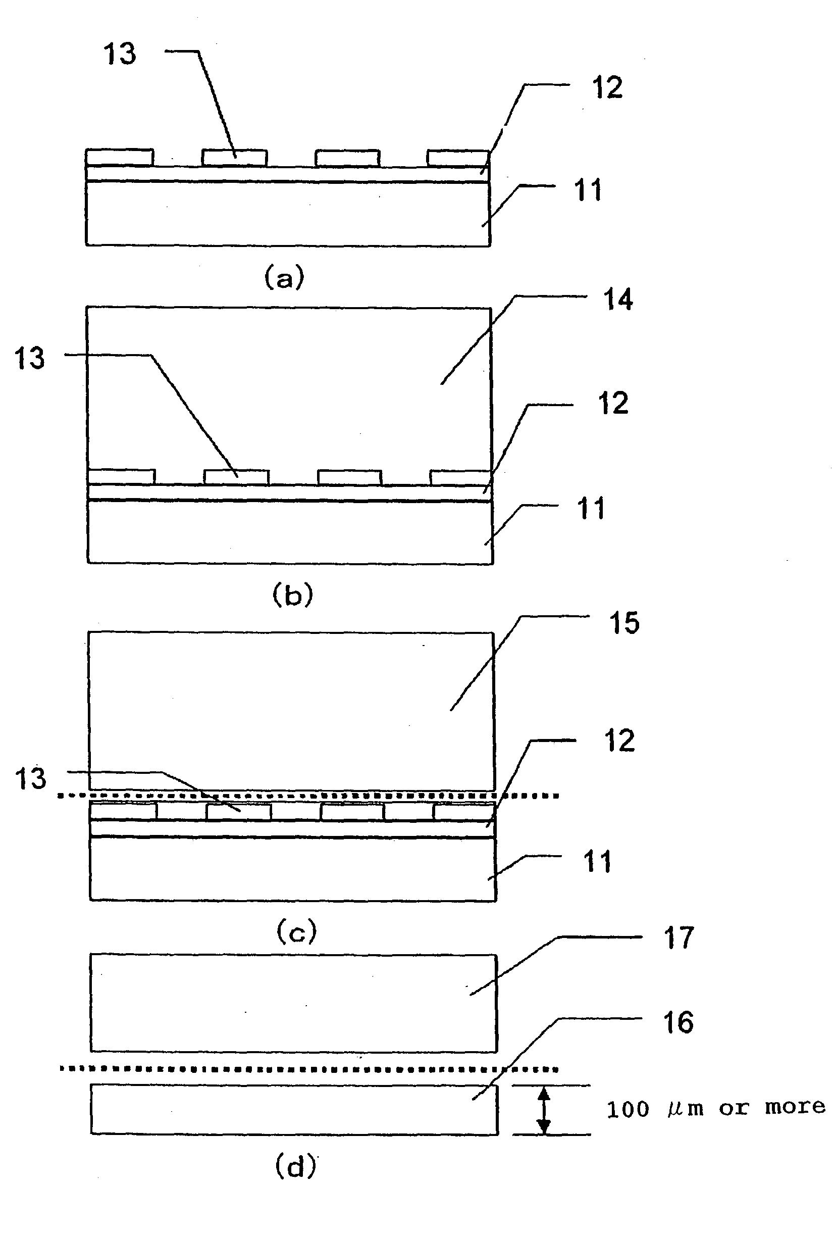
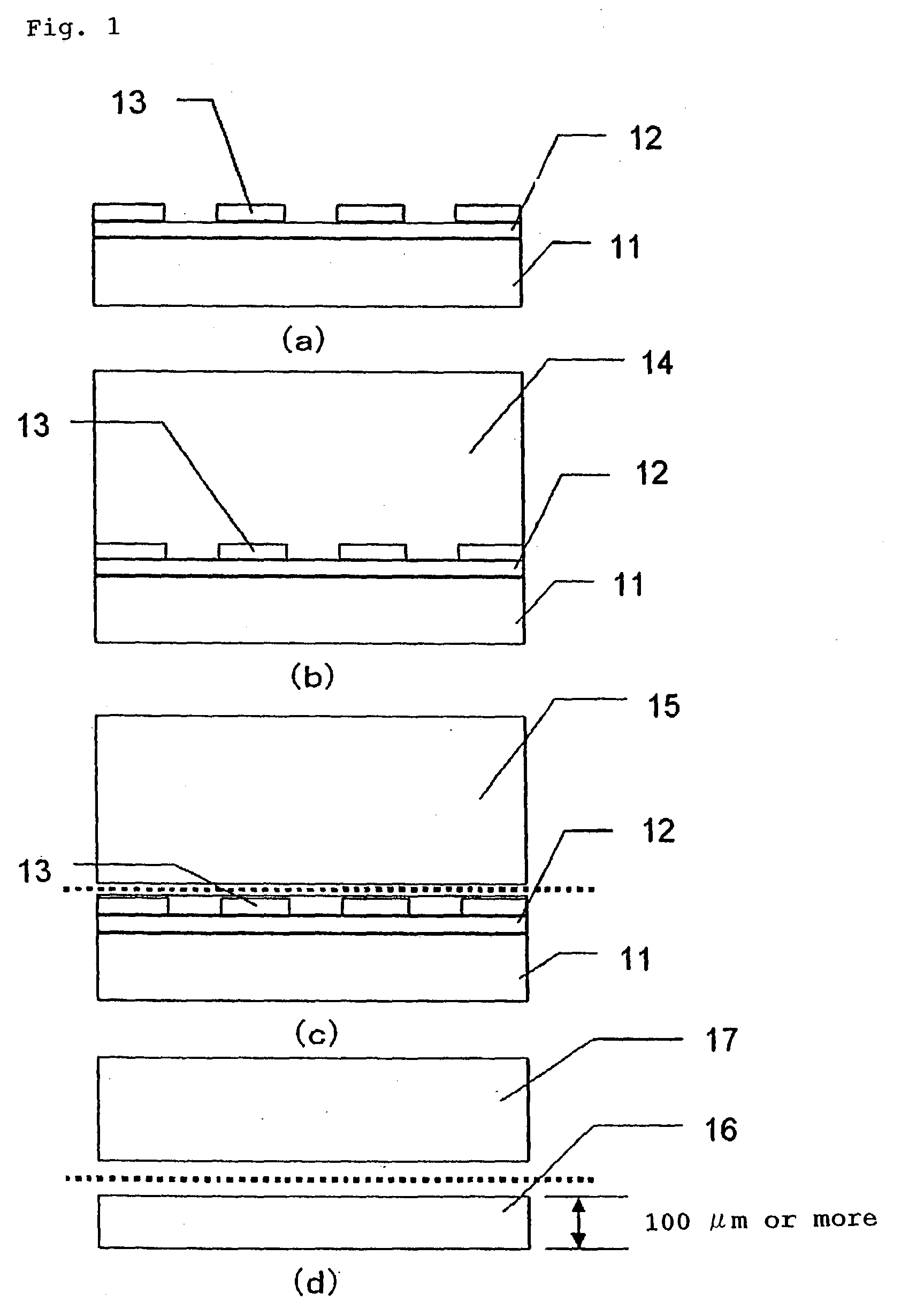
[0072] In the present example, the dislocation densities of the surfaces of a self-supporting substrate were controlled by a heat treatment. Referring to FIG. 3, a process for manufacturing a self-supporting GaN substrate according to the present example is explained below.

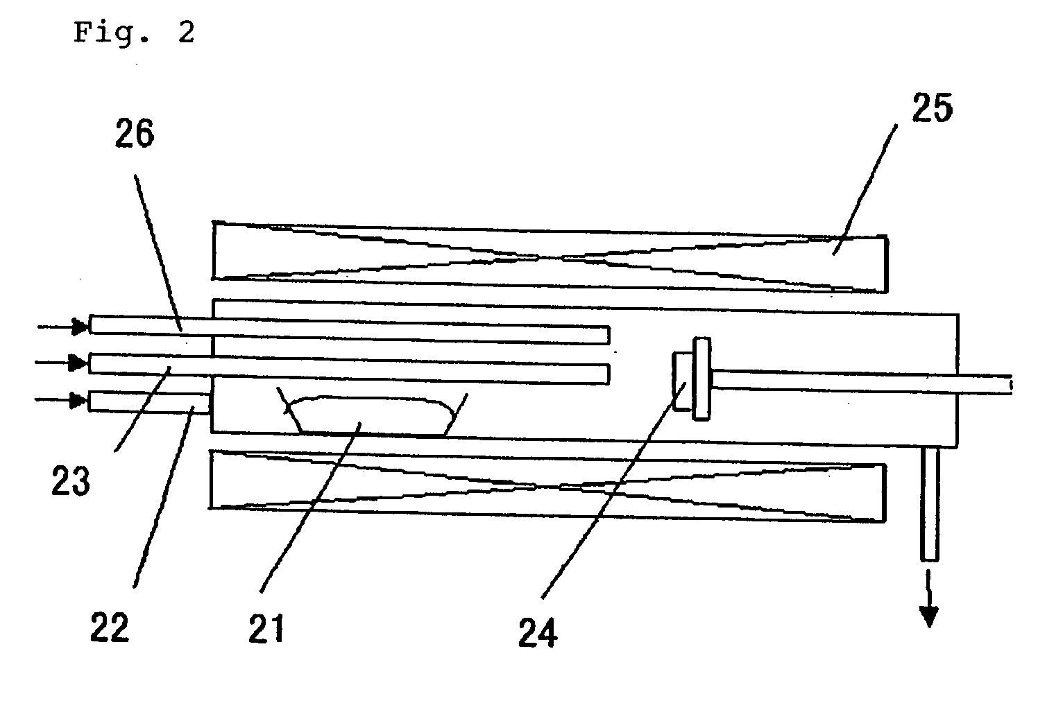
[0073] First, using a sapphire substrate 31, a GaN layer 33 was formed on a GaN low temperature growth buffer layer 32 with the afore-mentioned HVPE growth apparatus of FIG. 2 (FIG. 3(a)). In the substrate area inside of the apparatus, GaCl and NH.sub.3 that was supplied through a supply tube 23 were mixed, and, while interacting, formed GaN on a substrate 24 by vapor deposition. The temperature of the substrate area was set to be at 1000.degree. C. using an electric furnace 25. Further, the partial pressures of GaCl and NH.sub.3, both of which were the source gases, were 5.times.10.sup.-3 atm and 0.3 atm, respectively. Under these conditions, the growth rate thereof was approximately 50 am / h. Further, Doping was ...


PUM

PropertyMeasurementUnit
thicknessaaaaaaaaaa
thicknessaaaaaaaaaa
temperatureaaaaaaaaaa

Abstract

To provide a semiconductor substrate of a group III nitride with a little warp, this invention provides a process comprising such steps of: epitaxial-growing a GaN layer 33 with a GaN low temperature grown buffer layer 32 upon a sapphire substrate 31; removing the sapphire substrate 31, the GaN buffer layer 32 and a small portion of the GaN layer 33 from the substrate taken out of a growth reactor to obtain a self-supporting GaN substrate 35; and after that, heat-treating the GaN substrate 35 by putting it into an electric furnace under the NH3 atmosphere at 1200° C. for 24 hours; which leads to a marked reduction of the warp of the self-supporting GaN substrate 35 such that dislocation densities of its obverse and reverse surface are 4x10<7 >cm<-2 >and 8x10<5 >cm<-2>, and thereby such a low ratio of dislocation densities of 50 is well-controlled.

Description

[0001] The present invention relates to a group III nitride based semiconductor substrate and a process for manufacture thereof.BACKGROUND TO THE INVENTION[0002] Since the nitride semiconductor material is known to have a sufficiently large band gap and besides its inter-band transition is of direct transition type, many investigations for utilizing the nitride semiconductor material in the short wavelength light emission device are underway. Furthermore, as its saturation drift velocity of electrons is high and the two-dimensional carrier gas is available in their hetero-junction, the nitride semiconductor material is also regarded to be highly applicable to the electron device.[0003] The nitride semiconductor layer to constitute these devices can be obtained by epitaxial growth on a base substrate with the vapor phase deposition method such as metal-organic vapor phase epitaxy (MOVPE) method, molecular beam epitaxy (MBE) method or hydride vapor phase epitaxy (HVPE) method. However...

Claims


Application Information

Patent Timeline
Patent Type & Authority Applications(United States)
IPC IPC(8): C30B29/38C30B33/00H01L21/20H01L21/205H01L33/32H01S5/323
CPCC30B29/403C30B29/406C30B33/00H01L21/0242H01L21/02458Y10T428/265H01L21/0262H01L21/02639H01L21/0265H01L21/02664H01L21/0254H01L21/20
Inventor USUI, AKIRASHIBATA, MASATOMOOSHIMA, YUICHI
Owner SUMITOMO CHEM CO LTD
Why Eureka
Try Eureka