Deep-UV light-emitting diode and preparation method thereof

A light-emitting diode, deep ultraviolet technology, applied in the direction of semiconductor devices, electrical components, circuits, etc., can solve the problem that it is difficult to obtain a smooth surface

Inactive Publication Date: 2009-12-16
PEKING UNIV
View PDF0 Cites 50 Cited by
  • Summary
  • Abstract
  • Description
  • Claims
  • Application Information

AI Technical Summary

Problems solved by technology

It is also reported in the literature that the high-temperature GaN insertion layer is used to replace the AlN/AlGaN superlattice to block the threading dislocations extending from the AlN layer to the AlGaN and quantum wells, but the

Method used


Image

  • Deep-UV light-emitting diode and preparation method thereof
  • Deep-UV light-emitting diode and preparation method thereof
  • Deep-UV light-emitting diode and preparation method thereof

Examples


Embodiment 1

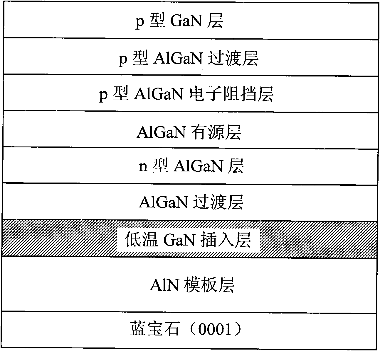
[0036] Deep-UV LEDs were fabricated by metal-organic chemical vapor deposition (MOCVD) according to the following steps:

[0037] 1) Raise the temperature of the reaction chamber to 1060°C, and heat and bake the sapphire substrate in a hydrogen atmosphere for 15 minutes;

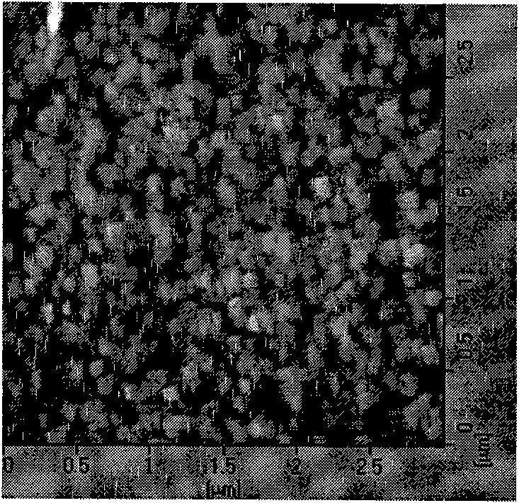
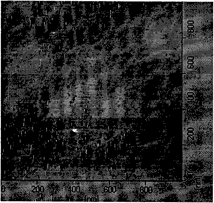
[0038] 2) Raise the temperature to 1200°C to grow a 320nm AlN template layer, growth conditions: pressure 50torr, V / III 600;

[0039] 3) Lower the temperature to 500°C, and grow a 20nm low-temperature GaN insertion layer on the basis of step 2), growth conditions: temperature 500°C, pressure 75torr, V / III 1500;

[0040] 4) Raise the temperature to 1150°C at a rate of 1°C per second, and grow 70nm Al on the basis of step 3) 0.7 Ga 0.3 The N layer is used as a transition layer, the growth pressure is 75torr, V / III 1500;

[0041] 5) keep the temperature constant, and grow 1 μm n-type Al on the basis of step 4) 0.6 Ga 0.4 The N layer is used as the n-type contact layer, the growth pressure is 75 torr, V / III...

Embodiment 2

[0050] Deep-UV LEDs were fabricated by metal-organic chemical vapor deposition (MOCVD) according to the following steps:

[0051] 1) Raise the temperature of the reaction chamber to 1060°C, and heat and bake the sapphire substrate in a hydrogen atmosphere for 15 minutes;

[0052] 2) Raise the temperature of the reaction chamber to 1200°C, using TMAl and NH 3 A pulsed AlN buffer layer with a thickness of 100nm was grown for 100 cycles by the pulsed atomic layer epitaxy method alternately fed into the reaction chamber, the specific growth pressure was 150 torr, V / III was 600, and each cycle was 5s TMAl / 3s hydrogen gas / 5s NH 3 / 3s hydrogen;

[0053] 3) Increase the temperature to 1200°C, and grow a 320nm AlN template layer on the basis of step 2), with a growth pressure of 50torr and V / III 600;

[0054] 4) Lower the temperature to 500°C, grow a 20nm low-temperature GaN insertion layer on the basis of step 3), growth pressure 75torr, V / III 1500;

[0055] 5) Raise the temperatu...


PUM

PropertyMeasurementUnit
Thicknessaaaaaaaaaa
Thicknessaaaaaaaaaa
Surface roughnessaaaaaaaaaa

Abstract

The invention provides a deep-UV light-emitting diode and a preparation method thereof. A low-temperature GaN insertion layer is used to replace an AlN/AlGaN superlattice or a high-temperature GaN insertion layer to grow the deep-UV light-emitting diode. The low-temperature GaN insertion layer is a GaN with thickness of 20-50nm under the conditions of temperature being 400-900 DEG C, pressure being 30-200torr, and V/III being 1500-2500. The method can effectively lower the dislocation density in an epitaxial AlGaN layer and a quantum well, and improves the surface planeness. The prepared LED component has smooth surface, better crystal quality, starting voltage reduction, and smaller serial resistances of the component; and the electroluminescene peak value is ranged from 300nm to 370nm.

Description

technical field [0001] The invention relates to the technical fields of semiconductor lighting and metal organic chemical vapor deposition (MOCVD), in particular to a short-wavelength AlGaN-based quantum well light-emitting diode (LED) and a preparation method thereof. Background technique [0002] Group III nitride materials are important wide-bandgap semiconductor materials with wide bandgap range (0.9eV-6.2eV), high breakdown electric field, high thermal conductivity, high electron saturation rate, strong radiation resistance and chemical corrosion resistance And other characteristics, these excellent optical, electrical properties and excellent material chemical properties make III-nitride materials in blue, green, purple, ultraviolet and white light-emitting diodes (LED), short-wavelength laser diodes (LD), ultraviolet light detection It has broad application prospects in the fields of semiconductor devices such as devices and power electronic devices. At present, the ...

Claims


Application Information

Patent Timeline
IPC IPC(8): H01L33/00
Inventor 秦志新桑立雯杨志坚方浩于彤军张国义
Owner PEKING UNIV
Why Eureka
Try Eureka