Method for preparing LED chip with separate crystal grain vertical structure

An LED chip, vertical structure technology, applied in the direction of semiconductor devices, electrical components, circuits, etc., can solve the problems of difficult-to-process substrates, die geometry design constraints, increase chip costs, etc., to reduce post-process and dislocation density. Reduce and improve efficiency

Inactive Publication Date: 2006-07-12
DONGGUAN INST OF OPTO ELECTRONICS PEKING UNIV
View PDF0 Cites 31 Cited by
  • Summary
  • Abstract
  • Description
  • Claims
  • Application Information

AI Technical Summary

Problems solved by technology

For GaN-based devices on sapphire substrates, the shape of the chip is limited due to the difference between the cleavage plane of sapphire and the GaN epitaxial layer, which restricts the design of the die geometry that is conducive to light extraction.
In addition, the use of difficult-to-process substrates increases the cost of chip fabrication

Method used


Image

  • Method for preparing LED chip with separate crystal grain vertical structure
  • Method for preparing LED chip with separate crystal grain vertical structure
  • Method for preparing LED chip with separate crystal grain vertical structure

Examples


Embodiment 1

[0049] Figure 3(a)-(f) shows the fabrication process of the discrete grain vertical structure light-emitting diode chip. In the figure, 1 indicates a sapphire substrate or a substrate with a GaN growth layer, and 2 indicates SiO 2 , 3 is an LED epitaxial wafer, 4 is a transparent electrode (Ni / Au), 5 is a reflective layer, 6 is a supporting substrate (Si or Cu), and 7 is a bonding metal (Au-Sn alloy). Below in conjunction with accompanying drawing, describe preferred embodiment one concrete steps in detail:

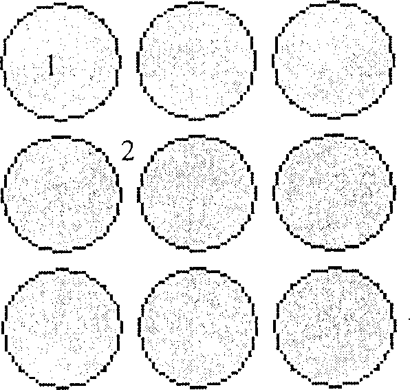
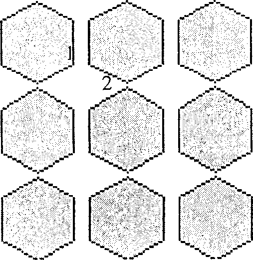
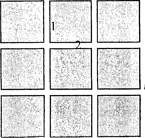
[0050] (a) Deposit SiO on sapphire substrate 1 2 2, and etch SiO 2 2 to define the island growth area and geometry. The size of the growth area is the size of the LED device, and the geometry of the growth area is polygonal and circular, which are conducive to light export. Figure 1 illustrates rectangles, hexagons and circles;

[0051] (b) On the substrate obtained in step (a), use MOCVD technology to grow the LED epitaxial layer, and perform P-type activation anneali...


PUM


Abstract

The invention presents a tube core shape design with high luminous efficiency, which comprises: epitaxial growing on island area LED chip with discrete grain; after laser peeling, packaging discrete chip into LED with vertical structure and high luminous efficiency. Wherein, the epitaxial growth improves crystal quality and internal quantum efficiency; the shape of island area increases LED light power; the island growth benefits to release stress, reduce stress on interface between GaN and sapphire substrate and the damage and spectral shift during peeling, thereby, it can obtain LED with high performance.

Description

technical field [0001] The invention belongs to the field of optoelectronic technology, and specifically relates to a method for preparing a power-type semiconductor light-emitting diode (LED) chip in combination with metal organic chemical vapor deposition (MOCVD) epitaxial growth technology, laser lift-off and reverse packaging technology. The invention proposes a method for directly obtaining discrete grain LED chips through growth, provides a new way for the geometric design of the LED chip not to be limited by the post-process of the LED chip, and is suitable for the preparation of new-type and high-power LEDs. Background technique [0002] Usually, LED is obtained by epitaxial growth on the substrate, thus, the preparation of LED is restricted by the crystal lattice structure of the substrate. The differences in lattice mismatch and thermal expansion coefficient cause a large number of dislocations due to the accumulation and release of stress in the epitaxial layer of...

Claims


Application Information

Patent Timeline
Patent Type & Authority Applications(China)
IPC IPC(8): H01L33/00
Inventor 于彤军秦志新杨志坚胡晓东陈志忠祁山陆羽康香宁商淑萍童玉珍丁晓民张国义
Owner DONGGUAN INST OF OPTO ELECTRONICS PEKING UNIV
Why Eureka
Try Eureka