Method for preparing LED chip with separate crystal grain vertical structure
A LED chip and vertical structure technology, applied in semiconductor devices, electrical components, circuits, etc., can solve problems such as difficult substrate processing, increased chip cost, and die geometry design constraints, so as to reduce post-processing, improve efficiency, Effect of Dislocation Density Reduction
- Summary
- Abstract
- Description
- Claims
- Application Information
AI Technical Summary
Problems solved by technology
Method used
Image
Examples
Embodiment 1
[0049] Figure 3(a)-(f) shows the fabrication process of the discrete grain vertical structure light-emitting diode chip. In the figure, 1 indicates a sapphire substrate or a substrate with a GaN growth layer, and 2 indicates SiO 2 , 3 is an LED epitaxial wafer, 4 is a transparent electrode (Ni / Au), 5 is a reflective layer, 6 is a supporting substrate (Si or Cu), and 7 is a bonding metal (Au-Sn alloy). Below in conjunction with accompanying drawing, describe preferred embodiment one concrete steps in detail:
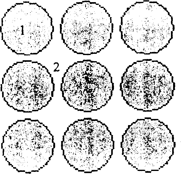
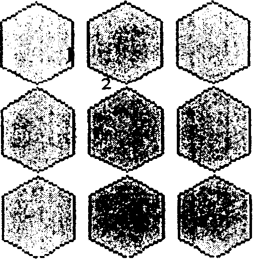
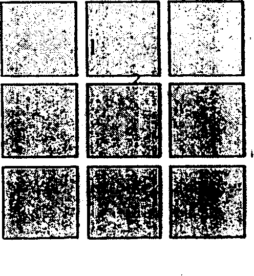
[0050] (a) Deposit SiO on sapphire substrate 1 2 2, and etch SiO 2 2 to define the island growth area and geometry. The size of the growth area is the size of the LED device, and the geometry of the growth area is polygonal and circular, which are conducive to light export. Figure 1 illustrates rectangles, hexagons and circles;
[0051] (b) On the substrate obtained in step (a), use MOCVD technology to grow the LED epitaxial layer, and perform P-type activation annea...
PUM
 Abstract
Description
Claims
Application Information


