Semiconductor light-emitting device, manufacturing method thereof, and lamp

a semiconductor and light-emitting technology, applied in semiconductor devices, current collectors, solid-state devices, etc., can solve the problems of difficult growth of deterioration of the crystallinity of the semiconductor layer of the led structure, and difficulty in growing a group iii nitride semiconductor layer having excellent crystallinity. , to achieve excellent crystallinity, the effect o

Active Publication Date: 2012-05-10
TOYODA GOSEI CO LTD
View PDF0 Cites 32 Cited by
  • Summary
  • Abstract
  • Description
  • Claims
  • Application Information

AI Technical Summary

Benefits of technology

[0011]Accordingly, an object of the present invention is to provide a semiconductor light-emitting device which includes a projection portion on a c-plane surface of a substrate and a semiconductor layer having excellent crystallinity on the substrate and is capable of providing a lamp having a small output decrease in a high temperature environment.
[0012]It is another object of the present invention to provide a manufacturing method of a semiconductor light-emitting device which is capable of providing a lamp having a small output decrease in a high temperature environment.
[0013]It is still another object of the present invention to provide a lamp including such a semiconductor light-emitting device, with a small output decrease in a high temperature environment.
[0023]The semiconductor light-emitting device according to the present invention includes: the single-crystal substrate, comprised c-plane main surface having a c-plane surface and a plurality of projection portions which are formed on the c-plane main surface of the single-crystal substrate; the intermediate layer which is formed to cover the main surface of the single-crystal substrate and includes AlN having the single-crystal phase on the c-plane surface and the polycrystalline phase on the projection portion wherein the film thickness t2 on the projection portion is smaller than the film thickness t1 on the c-plane surface (t2<t1), and the film thickness t2 on the projection portion is 60% or more of the film thickness t1 on the c-plane surface; and the semiconductor layer which is formed on the intermediate layer and includes the group III nitride semiconductor. Thus, a dislocation density of the semiconductor layer formed on the intermediate layer is decreased, and the crystallinity of the semiconductor layer is improved. Here, the film thickness t2 of the intermediate layer formed on the projection portion of the single-crystal substrate is smaller than the film thickness t1 of the intermediate layer formed on the c-plane surface, and thus, the relationship of t2<t1 is established. As a result, the semiconductor light-emitting device according to the present invention can form a lamp which has a small output decrease at a high temperature environment and excellent temperature characteristics.
[0025]More specifically, since the intermediate layer is formed under the condition that the relationship of D / H>d / h is established in the intermediate layer forming step, sputtering particles enter over a wide incident angle range in an entire area of the single-crystal substrate, the intermediate layer is also formed at a sufficiently thick thickness on the projection portion in a similar way to the c-plane surface regardless of the position on the single-crystal substrate, the ratio of the thickness on the projection portion and the thickness on the c-plane surface on the single-crystal substrate is within the specific range, and the intermediate layer having the single-crystal phase on the c-plane surface and the polycrystalline phase on the projection portion is obtained. As a result, according to the manufacturing method of the semiconductor light-emitting device according to the present invention, the dislocation density of the semiconductor layer formed on the intermediate layer is decreased, and the crystallinity of the semiconductor layer is improved.
[0026]Furthermore, the lamp according to the present invention includes the semiconductor light-emitting device according to the present invention in which the semiconductor layer has excellent crystallinity, and thus, has a small output decrease in a high temperature environment.

Problems solved by technology

However, in a case where recesses and projections are formed on a surface of a sapphire substrate and a group III nitride semiconductor layer is epitaxially grown thereon, it is difficult to grow a group III nitride semiconductor layer having excellent crystallinity.
For example, in a case where a projection portion is formed on a c-plane surface of a sapphire substrate and a group III nitride semiconductor layer which includes GaN of a single-crystal is epitaxially grown thereon, a crystalline defect such as dislocation tends to occur in a portion in which a semiconductor layer grown from a top portion of the projection portion and a semiconductor layer grown from the c-plane surface disposed around a base portion of the projection portion are merged, thereby making it difficult to grow a semiconductor layer having excellent crystallinity.
Thus, if the crystallinity of the group III nitride semiconductor layer grown on the substrate is not good, the crystallinity of the semiconductor layer of the LED structure also deteriorates.
As a result, in a case where the recesses and projections are formed on the surface of the sapphire substrate, although light extraction efficiency of the light-emitting device is enhanced, an output decrease in a high temperature environment is noticeable.

Method used


Image

  • Semiconductor light-emitting device, manufacturing method thereof, and lamp
  • Semiconductor light-emitting device, manufacturing method thereof, and lamp
  • Semiconductor light-emitting device, manufacturing method thereof, and lamp

Examples


example 1

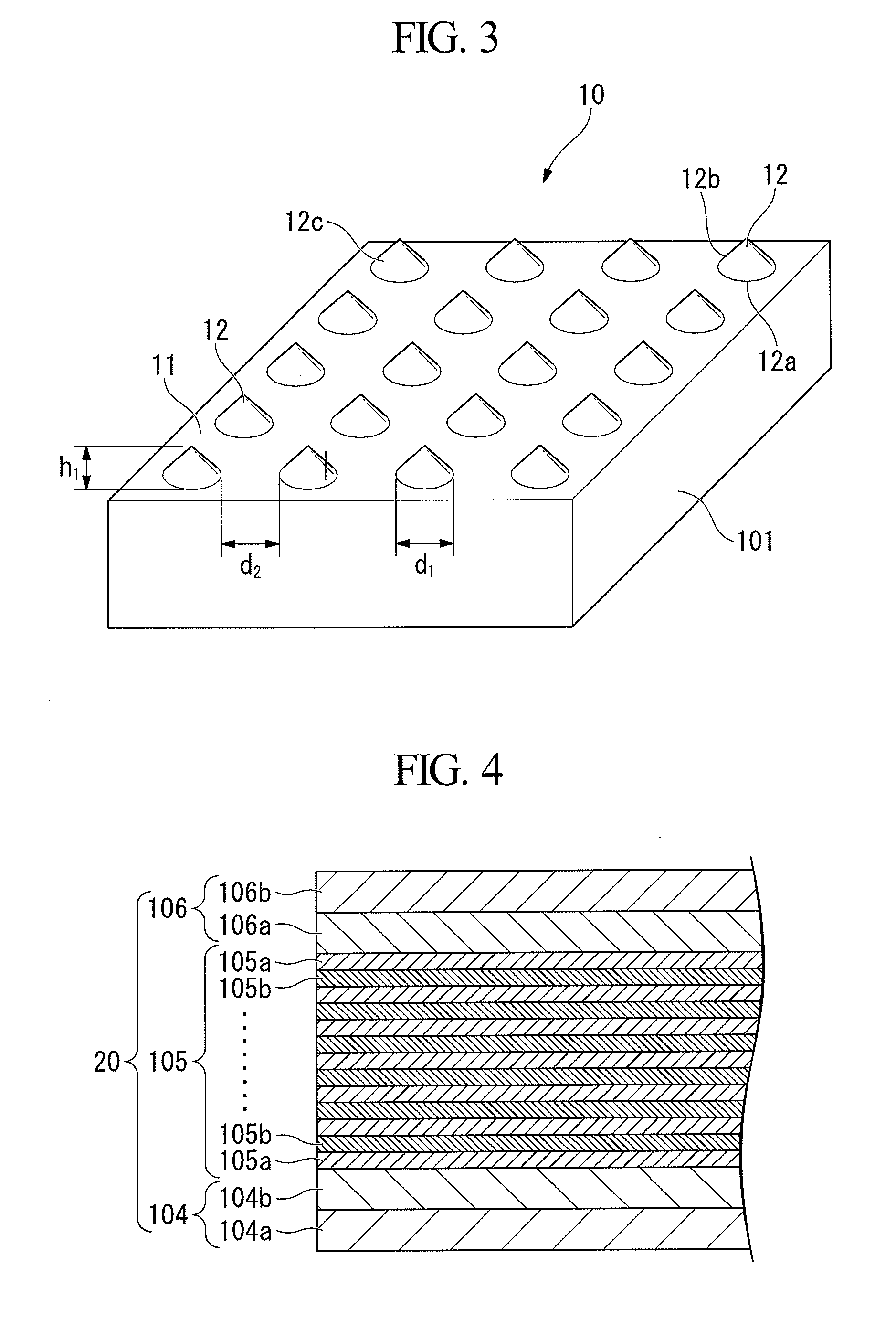
[0138]The plurality of projection portions having the “base width”, “height”, “base width / 4”, and “interval between adjacent projection portions” shown in Table 1 and the shape shown in Table 2 was formed on the (0001) c-plane surface of a sapphire substrate having a diameter of 100 mm (diameter of 4 inches) as follows (substrate processing process). Here, a mask was formed using known photolithography on the c-plane surface of sapphire substrate of the diameter of 4 inches, the sapphire substrate was etched using dry etching, to thereby form the projection portions. As an exposure method, a stepper exposure method using ultraviolet light was used. Furthermore, a mixed gas of BCl3 and Cl2 was used for the dry etching.

TABLE 1BaseInterval betweenBase width dHeight hwidth / 4adjacent projection(μm)(μm)(μm)portions (μm)Example 11.20.60.30.5Example 21.50.60.40.5Example 32.50.80.61.5Example 41.50.40.40.2Example 51.50.60.40.5Comparative1.50.60.40.5Example 1Comparative1.50.60.40.5Example 2

TAB...

example 2 to example 4

[0169]Light-emitting devices of Examples 2 to 4 were formed in the same manner as in Example 1 except that the plurality of projection portions having the “base width”, “height”, “base width / 4”, and “interval between adjacent projection portions” shown in Table 1 and the shape shown in Table 2 was formed on the (0001) c-plane surface of the sapphire substrate, and the light emission characteristics (temperature characteristics) were evaluated in the same way as in Example 1. The result is shown in Table 3.

[0170]Furthermore, the film thickness on the projection portion of the intermediate layer and the film thickness on the c-plane surface, whether the crystal phase on the c-plane surface and the projection portion is the single-crystal phase or the polycrystalline phase are shown in Table 2.

example 5

Comparative Example 1 and Comparative Example 2

[0171]Light-emitting devices of Example 5 and Comparative Examples 1 and 2 were formed in the same manner as in Example 1 except that the plurality of projection portions having the “base width”, “height”, “base width / 4”, and “interval between adjacent projection portions” shown in Table 1 and the shape shown in Table 2 was formed on the (0001) c-plane surface of the sapphire substrate and the intermediate layer was formed under the condition shown in Table 2, and the light emission characteristics were evaluated in the same way as in Example 1. The result is shown in Table 3.

[0172]Furthermore, the film thickness on the projection portion of the intermediate layer and the film thickness of the c-plane surface, whether the crystal phase on the c-plane surface and the projection portion is the single-crystal phase or the polycrystalline phase is shown in Table 2.

[0173]As shown in Table 2, in the light-emitting devices of Examples 1 to 5, ...


PUM


Abstract

A semiconductor light-emitting device which includes: a single-crystal substrate formed with a plurality of projection portions on a c-plane main surface; an intermediate layer which is formed to cover the main surface of the single-crystal substrate, in which a film thickness t2 on the projection portion is smaller than a film thickness t1 on the c-plane surface, in which the film thickness t2 on the projection portion is 60% or more of the film thickness t1 on the c-plane surface, and which includes AlN having a single-crystal phase on the c-plane surface and a polycrystalline phase on the projection portion; and a semiconductor layer which is formed on the intermediate layer and includes a group III nitride semiconductor.

Description

CROSS-REFERENCE TO RELATED APPLICATION[0001]This application claims priority of Japanese Patent Application No. 2010-249987 filed Nov. 8, 2010, the content of which is incorporated herein by reference in its entirety.BACKGROUND OF THE INVENTION[0002]1. Field of the Invention[0003]The present invention relates to a semiconductor light-emitting device, a manufacturing method thereof, and a lamp, and more particularly, to a semiconductor light-emitting device and a manufacturing method thereof which are capable of providing a lamp having a small output decrease in a high temperature environment.[0004]2. Description of Related Art[0005]As a semiconductor light-emitting device such as an LED (Light-Emitting Diode) used in a lamp, a technique has been used in which a group III nitride semiconductor layer is stacked on a sapphire single-crystal substrate.[0006]In recent years, as such a semiconductor light-emitting device, a technique has been proposed in which recesses and projections are...

Claims


Application Information

Patent Timeline
Patent Type & Authority Applications(United States)
IPC IPC(8): H01L33/22H01L33/16
CPCH01L21/0242H01L21/0243H01L2224/49107H01L2224/48257H01L2224/48247H01L21/02458H01L21/02513H01L21/0254H01L21/02576H01L21/02579H01L21/0262H01L21/02631H01L21/02639H01L33/007H01L33/12H01L33/20H01L33/32H01L2224/45144H01L2224/48091H01L2924/00014H01L2924/00
Inventor YOKOYAMA, YASUNORI
Owner TOYODA GOSEI CO LTD
Why Eureka
Try Eureka