III-V group nitride system semiconductor self-standing substrate, method of making the same and III-V group nitride system semiconductor wafer

a technology of iii-v group nitride and self-standing substrate, which is applied in the direction of polycrystalline material growth, crystal growth process, chemically reactive gas, etc., can solve the problems of inability to obtain the high-performance device desired currently, inability to obtain a high-quality grown layer, and large number of crystal defects, etc., to achieve less distortion, good crystalline quality, and less accumulation of distortion

Active Publication Date: 2006-02-16
SUMITOMO CHEM CO LTD
View PDF7 Cites 34 Cited by
  • Summary
  • Abstract
  • Description
  • Claims
  • Application Information

AI Technical Summary

Benefits of technology

[0091] By virtue of the self-standing substrate of the invention, when an epitaxial growth layer of nitride system semiconductor is grown on the III-V group nitride system semiconductor self-standing substrate, distortion is less likely to be accumulated. Along with this, an epitaxial growth layer with good crystalline quality can be obtained since temperature in growth interface is sufficiently uniformed during the crystal growth. Further, due to the less accumulation in distortion, it is less likely to occur that the substrate is split or chipped during the fabrication process.
[0092] Further, by virtue of the method of the invention, a III-V group nitride system semiconductor self-standing substrate can be obtained that has a low dislocation density and a substantially uniform dislocation density distribution at the surface, with stability and good reproducibility.
[0093] Further, by virtue of the invention, the III-V group nitride system semiconductor wafer can be provided with an epitaxial growth layer with enhanced crystalline quality, good uniformity and less accumulation in distortion. Therefore, in fabricating a device such as a light emitting device or electronic device, enhancement in device characteristics or production yield can be estimated.

Problems solved by technology

However, since there is no underlying substrate that has a lattice constant matched to that of nitride semiconductor layers, it is impossible to obtain a high quality of grown layer and therefore a number of crystal defects (dislocations) are generated in the resulting nitride semiconductor layers.
However, even when the method using the buffer layer is conducted, the resulting GaN film includes a considerable number of crystal defects such as a penetrating dislocation or a vacancy.
Thus, it is not a satisfactory method for obtaining a high-performance device desired currently.
However, in the case of GaN self-standing substrate, since thick GaN crystal epitaxially grown on a hetero-substrate is separated (peeled) from the hetero-substrate after the growth to obtain the GaN self-standing substrate, it is difficult to suppress the occurrence of dislocation near at the hetero-epitaxial growth interface corresponding to the initial stage of crystal growth.
Therefore, it was in fact impossible to obtain a substrate surface that gathered dislocations are perfectly dispersed, or a substrate surface obtainable when dislocations are uniformly dispersed was unintentionally removed by polishing at the substrate surface.

Method used


Image

  • III-V group nitride system semiconductor self-standing substrate, method of making the same and III-V group nitride system semiconductor wafer
  • III-V group nitride system semiconductor self-standing substrate, method of making the same and III-V group nitride system semiconductor wafer
  • III-V group nitride system semiconductor self-standing substrate, method of making the same and III-V group nitride system semiconductor wafer

Examples


first embodiment

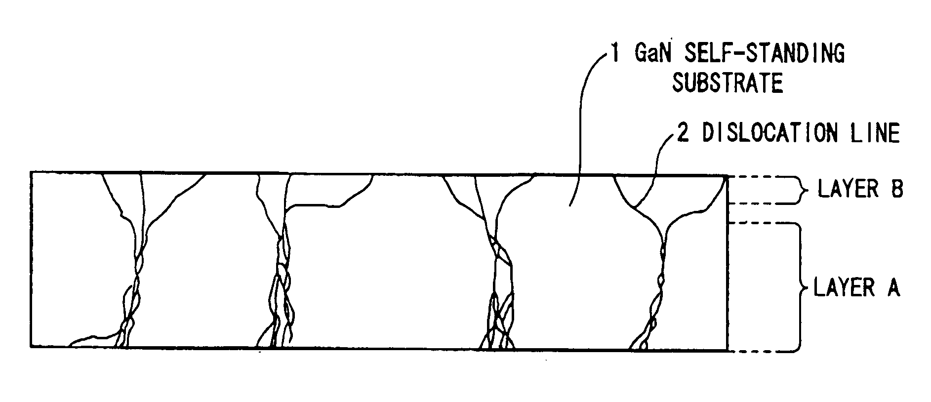
[0158] [Manufacturing of a GaN self-standing substrate that a layer with a substantially uniform dislocation density distribution is formed on a layer that has a region with dislocation lines gathered densely and a region with dislocation lines thinly gathered]

[0159] A GaN epitaxial layer is formed on a sapphire substrate, and then the sapphire substrate is removed. Thus, a GaN self-standing substrate is manufactured and evaluated that, as schematically shown in FIG. 3, layer B with a substantially uniform dislocation density distribution is formed on layer A that has a region with dislocation lines gathered densely and a region with dislocation lines thinly gathered.

[0160] Referring to FIGS. 4A to 4G, a method of making the GaN self-standing substrate in this embodiment of the invention will be explained below.

[0161] First, using a sapphire substrate 11 as shown in FIG. 4A, GaN crystal 12 is epitaxially grown by HVPE. The HVPE is a method that GaCl as III-group element halide is ...

second embodiment

[0183] [Manufacturing of a GaN self-standing substrate that a layer with a substantially uniform dislocation density distribution is formed on a layer that has a region with dislocation lines gathered densely and a region with dislocation lines thinly gathered]

[0184] Under the same conditions as the first embodiment except that the crystal growth conditions by HVPE is slightly changed, a GaN epitaxial layer is grown on a sapphire substrate. Then, by removing the sapphire substrate, a GaN self-standing substrate is obtained and evaluated that, as shown in FIG. 3, layer B with a substantially uniform dislocation density distribution is formed on layer A that has a region with dislocation lines gathered densely and a region with dislocation lines thinly gathered.

[0185] Referring to FIGS. 4A to 4G, a method of making the GaN self-standing substrate in the second embodiment of the invention will be explained below.

[0186] First, using a sapphire C-face substrate 11 as shown in FIG. 4A, ...

third embodiment

[0196] [Manufacturing by VAS of a GaN self-standing substrate that a layer with a substantially uniform dislocation density distribution is formed on a layer that has a region with dislocation lines gathered densely and a region with dislocation lines thinly gathered]

[0197] By using the VAS (void-assisted separation) method, a GaN epitaxial layer is grown on a sapphire substrate. Then, by removing the sapphire substrate, a GaN self-standing substrate is obtained and evaluated that a layer with a substantially uniform dislocation density distribution is formed on a layer that has a region with dislocation lines gathered densely and a region with dislocation lines thinly gathered. The VAS method is such a method that the crystal growth is conducted while sandwiching a titanium nitride thin film with a network structure between a sapphire substrate and a GaN growth layer, and is disclosed in Japanese patent application laid-open No. 2003-178984.

[0198] Referring to FIGS. 10A to 10G, a ...


PUM

PropertyMeasurementUnit
thicknessaaaaaaaaaa
thicknessaaaaaaaaaa
thicknessaaaaaaaaaa

Abstract

A III-V group nitride system semiconductor self-standing substrate has: a first III-V group nitride system semiconductor crystal layer that has a region with dislocation lines gathered densely, the dislocation lines being gathered substantially perpendicular to a surface of the substrate, and a region with dislocation lines gathered thinly; and a second III-V group nitride system semiconductor crystal layer that is formed up to 10 μm from the surface of the substrate on the first III-V group nitride system semiconductor crystal layer and that has a dislocation density distribution that is substantially uniform.

Description

[0001] The present application is based on Japanese patent application No. 2004-233701, the entire contents of which are incorporated herein by reference. BACKGROUND OF THE INVENTION [0002] 1. Field of the Invention [0003] The present invention relates to a III-V group nitride system semiconductor self-standing substrate and, in particular, to a III-V group nitride system semiconductor self-standing substrate with a uniform dislocation density distribution and a reduced dislocation on its surface, a method of making the same, and a III-V group nitride system semiconductor wafer with a nitride system semiconductor layer epitaxially grown on the substrate. [0004] 2. Description of the Related Art [0005] Nitride system semiconductor materials such as gallium nitride (GaN), indium gallium nitride (InGaN) and gallium aluminum nitride (GaAlN) have a sufficiently wide bandgap and are of direct transition type in inter-band transition. Therefore, they are a great deal researched to be used ...

Claims


Application Information

Patent Timeline
Patent Type & Authority Applications(United States)
IPC IPC(8): H01L21/00H01L33/00C30B29/38H01L21/205
CPCC30B25/02C30B25/18C30B29/403H01L21/0242H01L21/02458H01L21/02647H01L21/02502H01L21/02513H01L21/0254H01L21/0262H01L21/02639H01L21/02491
Inventor SHIBATA, MASATOMO
Owner SUMITOMO CHEM CO LTD
Why Eureka
Try Eureka