Epitaxial structure and growing method for improving gallium nitride (GaN) based light-emitting diode (LED) lighting efficiency

A technology of epitaxial structure and luminous efficiency, applied in electrical components, circuits, semiconductor devices, etc., can solve the problems of reducing the composition of In quantum dots, deteriorating the quality of quantum well crystals, reducing the luminous efficiency of devices, etc., to eliminate stress and crystal defects, The effect of improving internal quantum efficiency and luminous efficiency and improving crystal quality

Inactive Publication Date: 2013-04-24
合肥彩虹蓝光科技有限公司
View PDF4 Cites 50 Cited by
  • Summary
  • Abstract
  • Description
  • Claims
  • Application Information

AI Technical Summary

Problems solved by technology

However, after the growth of the InGaN potential well layer is completed, the GaN barrier layer is often grown at high temperature, which will lead to the volatilization of In and the change in the thickness direction of the potential well layer, thereby causing the reduction of the composition of In quantum dots and the expansion of the luminous wavelength.
In addition, the diffusion of Si atoms into the InGaN potential well layer will also cause the deterioration of the quantum well crystal quality and reduce the luminous efficiency of the device.

Method used


Image

  • Epitaxial structure and growing method for improving gallium nitride (GaN) based light-emitting diode (LED) lighting efficiency
  • Epitaxial structure and growing method for improving gallium nitride (GaN) based light-emitting diode (LED) lighting efficiency

Examples


Embodiment Construction

[0022] The embodiments of the present invention are described in detail below: the present embodiment is implemented under the premise of the technical solution of the present invention, and detailed implementation and specific operation process are provided, but the protection scope of the present invention is not limited to the following implementation example.

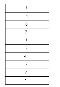
[0023] Such as figure 1 The LED epitaxial structure shown, from bottom to top, includes: substrate 1, low-temperature GaN buffer layer 2, GaN undoped layer 3, N-type GaN layer 4, multi-quantum well structure MQW5, multi-quantum well active layer 6. A low-temperature P-type GaN layer 7 , a P-type AlGaN layer 8 , a high-temperature P-type GaN layer 9 , and a P-type contact layer 10 .

[0024] A method for growing an epitaxial structure for improving the luminous efficiency of the gallium nitride-based LED, comprising the following specific steps:

[0025] Step 1: Clean the substrate 1 at a high temperature for 5-20 ...


PUM

PropertyMeasurementUnit
temperatureaaaaaaaaaa
thicknessaaaaaaaaaa
thicknessaaaaaaaaaa

Abstract

The invention discloses an epitaxial structure and a growing method for improving gallium nitride (GaN) based light-emitting diode (LED) lighting efficiency. The order of the epitaxial structure from bottom to up is that a substrate, a low-temperature GaN buffer layer, a GaN non-doping layer, a N-shaped GaN layer, a multiple quantum well (MQW) structure, a multiple quantum well active layer, a low-temperature P-shaped GaN layer, a P-shaped aluminum (AL) GaN layer, a high-temperature P-shaped GaN layer and a P-shaped contact layer, wherein the order of the multiple quantum well active layer from bottom to up comprises a InyGa1-yN potential well layer, a InN layer and a barrier layer in sequence. The growing method of the multiple quantum well active layer structure is that by inserting the InN layer and a low-temperature annealing step in the growing process of a InyGa1 potential well layer and a GaN barrier layer, so that the composition of In quantum dot in the barrier layer is advanced and crystalline quality of the quantum well is improved, therefore, gallium nitride based LED lighting efficiency is improved.

Description

[0001] technical field [0002] The invention relates to the technical field of preparation of group III nitride materials, in particular to a novel multi-quantum well active layer structure and an epitaxial growth method capable of effectively improving the luminous efficiency of gallium nitride-based light-emitting diodes. Background technique [0003] Light Emitting Diode (LED, Light Emitting Diode) is a semiconductor solid-state light-emitting device, which uses a semiconductor PN junction as a light-emitting material, and can directly convert electricity into light. When the forward voltage is applied to both ends of the semiconductor PN junction, the minority carriers injected into the PN junction recombine with the majority carriers, releasing excess energy to cause photon emission, and directly emit light of various colors. [0004] Group III nitrides represented by gallium nitride are wide-bandgap semiconductor materials with direct bandgap, which have excellent p...

Claims


Application Information

Patent Timeline
Patent Type & Authority Applications(China)
IPC IPC(8): H01L33/06H01L33/00
Inventor 李刚郭丽彬
Owner 合肥彩虹蓝光科技有限公司
Why Eureka
Try Eureka