Method of manufacturing a free-standing substrate made of monocrystalline semi-conductor material

a manufacturing method and semiconductor technology, applied in the direction of polycrystalline material growth, crystal growth process, chemically reactive gas, etc., can solve the problems of difficult implementation of conditions, poor crystalline quality obtained, and no manufacturing method for gan or aln ingots that can be used on an industrial development scale, so as to improve the crystal quality of the deposited third material

Inactive Publication Date: 2005-11-15
SOITEC SA
View PDF26 Cites 50 Cited by
  • Summary
  • Abstract
  • Description
  • Claims
  • Application Information

AI Technical Summary

Benefits of technology

[0020]The epitaxial growing of the substrate includes initially providing a fine nucleation layer on the nucleation layer in order to improve the crystal quality of the deposited third material. The fine nucleation layer may be provided by metal organic chemical vapor deposition (MOCVD) epitaxy or by molecular beam (MBE) epitaxy. If desired, the nucleation layer can be eliminated so that the substrate becomes a free-standing structure.

Problems solved by technology

Unfortunately, at the present time, there is no manufacturing method for GaN or AlN ingots that can be used on an industrial development scale.
The article “Bulk and homoepitaxial GaN growth and characterisation”, Porowski-S, Journal of Crystal Growth, Vol. 189-190, June 1998, pp 153-158, describes a process for growing monocrystalline GaN ingots in the liquid phase under a pressure of 12 to 20 kbars (12 to 20×108 Pa) and at a temperature of between 1400 and 1700° C. These conditions are difficult to implement, however, in the course of mass production.
Other teams of researchers have also worked on methods for growing ingots in liquid phase at reduced pressure (less than 2 bars (2×10⁵ Pa)) and at a temperature of 1000° C. The diameter of the crystals obtained is larger, in the vicinity of 50 mm, but the crystalline quality obtained is less satisfactory than in the previously mentioned method.
The manufacturing conditions used are a pressure of less than 1 bar (105 Pa) and a temperature of from 1000 to 1200° C. The crystal quality is very good but the size of the crystal is 3 mm, which is clearly inadequate for the intended applications in the semiconductor field.
However, the GaN plates obtained in this fashion have many residual stresses and tensions connected with heteroepitaxy.
However, removal of this SiC substrate is very time-consuming because it is chemically very inert.
Implementing this removal technique is delicate for treating large surfaces because the laser beam scanning is long.
It is also possible to remove the sapphire substrate by mechanical polishing but this method is likewise time-consuming and further presents the risk of breakage of the GaN layer at the time of removal of the substrate that releases the stresses.
This technique enables easy removal of the substrate, however, the latter is lost, which is less of an advantage from an economic point of view.
However, none of these four documents mention the possibility of placing a nucleation layer on a support by molecular adhesion bonding.

Method used


Image

  • Method of manufacturing a free-standing substrate made of monocrystalline semi-conductor material
  • Method of manufacturing a free-standing substrate made of monocrystalline semi-conductor material
  • Method of manufacturing a free-standing substrate made of monocrystalline semi-conductor material

Examples


example 1

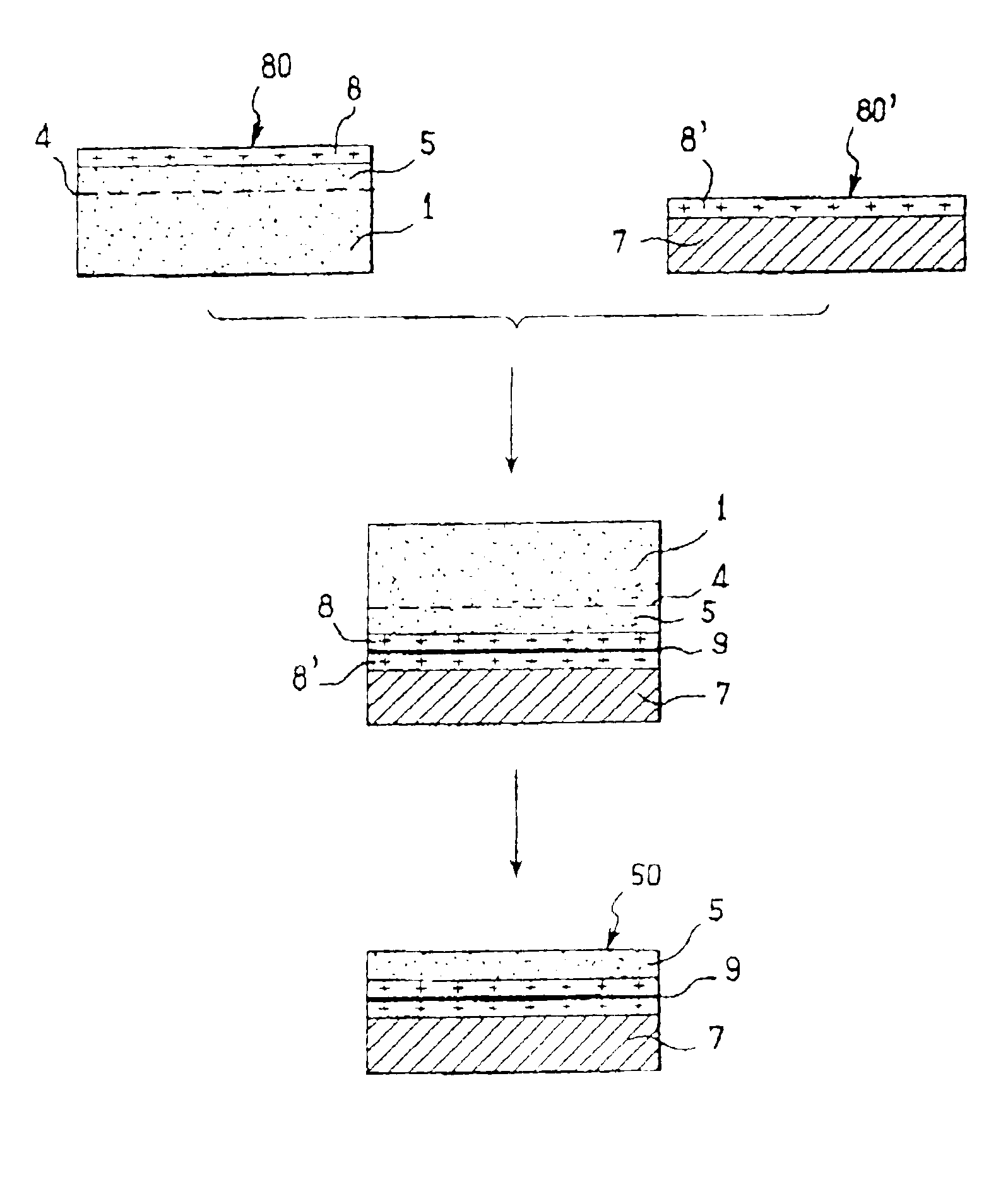
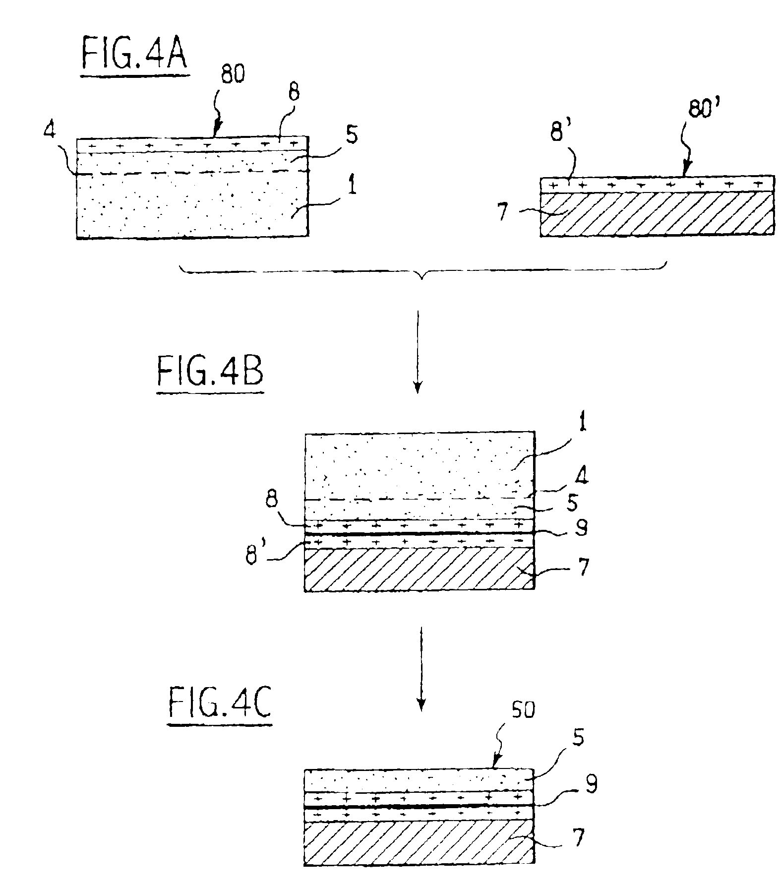
[0107]Manufacturing of a free-standing GaN substrate using an intermediate stack comprising a silicon Si support, two intermediate SiO2 / SiO2 bonding layers and a monocrystalline GaN nucleation layer.

[0108]A monocrystalline gallium nitride (GaN) nucleation layer 5 is formed in a solid source substrate 1 of solid GaN by ion implantation. This nucleation layer 5 is bonded onto a silicon mechanical support 7 by two intermediate bonding layers 8, 8′ of SiO2 bonded together along a bonding interface 9.

[0109]Prior to being assembled together, the two intermediate layers 8, 8′ undergo mechano-chemical planarization and surface treatment intended to increase roughness of the opposing surfaces 80, 80′ (e.g., a treatment with hydrofluoric acid HF or with a chemical cleaning solution known to the skilled artisan the name SC1 and comprised principally of ammonia diluted with hydrogen peroxide H2O2) of the opposing surfaces 80, 80′).

[0110]Then the nucleation layer 5 is detached from the rest of t...

example 2

[0118]Manufacturing of a free-standing AlN substrate using an intermediate stack comprising a silicon Si support, intermediate SiO2 / SiO2 bonding layers and a monocrystalline AlN nucleation layer.

[0119]One proceeds in identical fashion as described for Example 1, except that the solid gallium nitride is replaced by aluminum nitride (AlN) and that the different AlN layers have a coefficient of thermal expansion in the area of 4.15×10⁻¹⁶ / K, while the coefficient of thermal expansion of the silicon forming the support is 2.5×10⁻⁶ / K.

[0120]Removal is done likewise naturally by lowering the temperature of the stack.
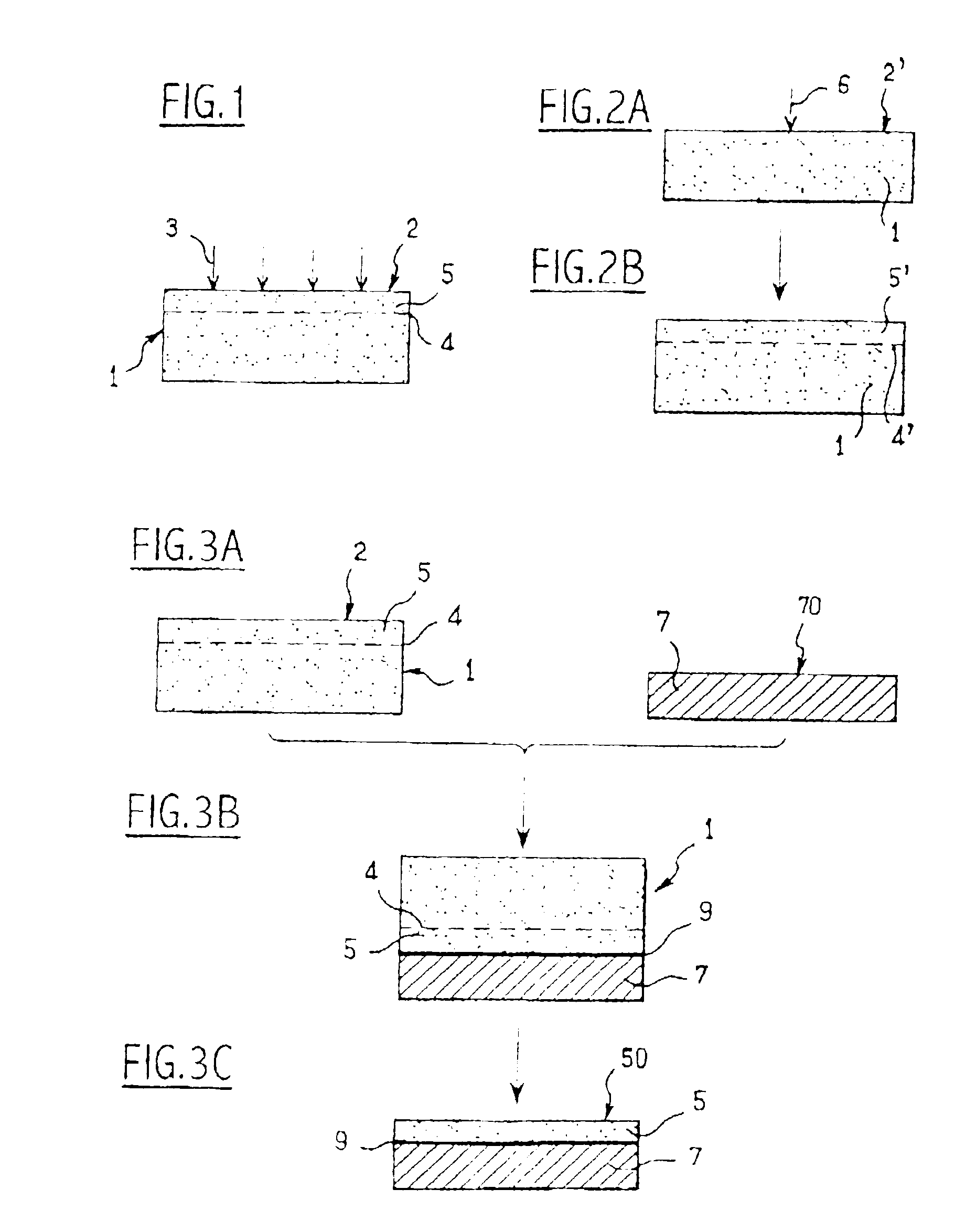
example 3

[0121]Manufacturing of a free-standing GaN substrate using an intermediate stack comprising a silicon support, a single intermediate bonding layer of SiO2 and a silicon Si {111} nucleation layer.

[0122]A nucleation layer 5 of silicon {111} is formed in a source substrate 1 of the same type by ion implantation. This nucleation layer 5 is bonded onto a silicon mechanical support 7 by an intermediate bonding layer 8 of SiO2 obtained by thermal oxidation of the top surface of the source substrate 1. The bonding interface 9 is disposed between the top surface 80 of the SiO2 layer and the frontal surface 2 of the nucleation layer 5.

[0123]This bonding interface 9 is treated as in Example 1 so as to be removable.

[0124]Then the nucleation layer 5 is removed from the rest of the source substrate 1 along the embrittled zone 4.

[0125]A finishing step is then operated on the exposed surface 50 of the nucleation layer 5.

[0126]Then fast growth of a GaN layer 10 by HVPE at 1050° C. is realized. At th...


PUM

PropertyMeasurementUnit
thicknessaaaaaaaaaa
thicknessaaaaaaaaaa
diameteraaaaaaaaaa

Abstract

A method for manufacturing a free-standing substrate made of a semiconductor material. A first assembly is provided and it includes a relatively thinner nucleation layer of a first material, a support of a second material, and a removable bonding interface defined between facing surfaces of the nucleation layer and support. A substrate of a relatively thicker layer of a third material is grown, by epitaxy on the nucleation layer, to form a second assembly with the substrate attaining a sufficient thickness to be free-standing. The third material is preferably a monocrystalline material. Also, the removable character of the bonding interface is preserved with at least the substrate being heated to an epitaxial growth temperature. The coefficients of thermal expansion of the second and third materials are selected to be different from each other by a thermal expansion differential, determined as a function of the epitaxial growth temperature or subsequent application of external mechanical stresses, such that, as the second assembly cools from the epitaxial growth temperature, stresses are induced in the removable bonding interface to facilitate detachment of the nucleation layer from the substrate.

Description

BACKGROUND ART[0001]This invention relates to a method for manufacturing a free-standing substrate made of mono-crystalline semiconductor material, in particular a wide bandgap material, and in particular for manufacturing a substrate comprised of gallium nitrate (GaN), aluminum nitrate (AlN) or diamond.[0002]A free-standing substrate is defined as a substrate, whose thickness is sufficient that it carries itself without support. Reasonably, such a substrate must thus have a thickness of at least 100 μm. However, in order to be able to be manipulated in a manufacturing line without risk of breaking, it must generally be thicker.[0003]By way of example, the commercially available free-standing substrates comprised of GaN or AlN have a thickness of 300 μm. Such free-standing substrates comprised of GaN or AlN are used in opto-electronic devices such as LEDs, lasers, sensors or in micro-electronic devices (transistors) or function in a high-temperature environment, or even in the field...

Claims


Application Information

Patent Timeline
Patent Type & Authority Patents(United States)
IPC IPC(8): H01L21/762H01L21/20H01L21/70H01L21/02C23C16/01C23C16/34C30B25/02C30B29/04C30B29/38
CPCH01L21/76254Y10S438/977C30B29/40
Inventor GHYSELEN, BRUNOLETERTRE, FABRICEMAZURE, CARLOS
Owner SOITEC SA
Why Eureka
Try Eureka