Semiconductor light emitting element and method for manufacturing same, integrated semiconductor light-emitting device and method for manufacturing same, image display and method for manufacturing same, and illuminating device and method for manufacturing same

a technology of semiconductor light-emitting devices and semiconductor light-emitting elements, which is applied in the direction of water treatment parameter control, separation processes, coatings, etc., can solve the problems of large occupied area per element, unsatisfactory light-emitting efficiency, etc., and achieve the effect of reducing the size of the light-emitting element structure, efficient extraction, and reducing the size of the crystal portion

Inactive Publication Date: 2005-07-07
SONY CORP
View PDF10 Cites 54 Cited by
  • Summary
  • Abstract
  • Description
  • Claims
  • Application Information

AI Technical Summary

Benefits of technology

[0101] According to the invention having the above-summarized configuration, the semiconductor layer of the first conduction type is selectively grown under the existence of the growth mask having the opening in a predetermined portion. Thereby, it is possible to make a convex crystal portion having an inclined crystal plane composed of a plurality of crystal planes different in angle of inclination to exhibit a good convex plane as a whole or having an inclined crystal exhibiting a substantially convex plane as a whole. Then, by sequentially growing at least the active layer and the semiconductor layer of the second conduction type to cover the crystal plane, the light emitting element structure can be formed. In this case, the semiconductor layer of the second conduction type also has an inclined crystal plane composed of a plurality of crystal planes different in angle of inclination to exhibit a good convex plane as a whole, or an inclined crystal plane exhibiting a substantially convex plane as a whole. Therefore, in operation of the element, light generated from the active layer can be extracted efficiently by reflection at the inclined crystal plane of the semiconductor layer of the second conduction type, which exhibits the convex plane or the substantially convex plane. Moreover, in comparison with a structure in which the crystal portion has an S-oriented inclined crystal plane, the present invention can diminish the size of the crystal portion and can therefore reduce the size of the light emitting element structure made by sequentially growing the active layer and the semiconductor layer of the second conduction type on the crystal portion. Furthermore, since the light extracting direction can be closer to the direction normal to the major plane, light is less subjected to blockage even when a black mask, or the like, is placed in the portion other than the light emitting portion.

Problems solved by technology

Existing semiconductor light emitting elements, having a light emitting element structure made by selectively growing the six-sided pyramidal n-type GaN layer 105 having an S-oriented inclined crystalline plane and next growing the active layer 106 and the p-type GaN layer 107 on the S-oriented plane, were unsatisfactory in light emitting efficiency, and inevitably required a large occupied area per each element.

Method used


Image

  • Semiconductor light emitting element and method for manufacturing same, integrated semiconductor light-emitting device and method for manufacturing same, image display and method for manufacturing same, and illuminating device and method for manufacturing same
  • Semiconductor light emitting element and method for manufacturing same, integrated semiconductor light-emitting device and method for manufacturing same, image display and method for manufacturing same, and illuminating device and method for manufacturing same
  • Semiconductor light emitting element and method for manufacturing same, integrated semiconductor light-emitting device and method for manufacturing same, image display and method for manufacturing same, and illuminating device and method for manufacturing same

Examples


first embodiment

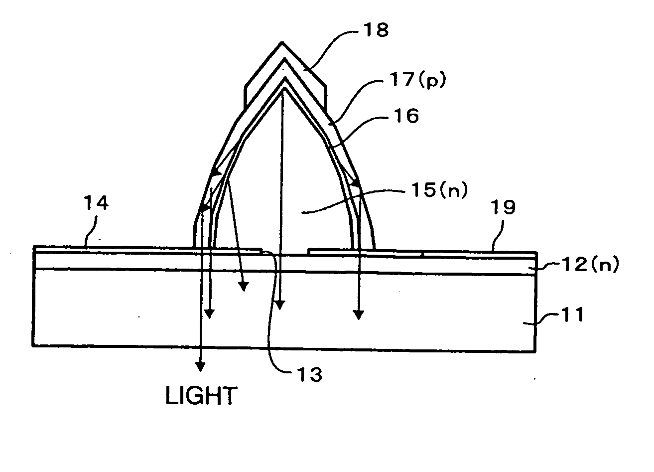
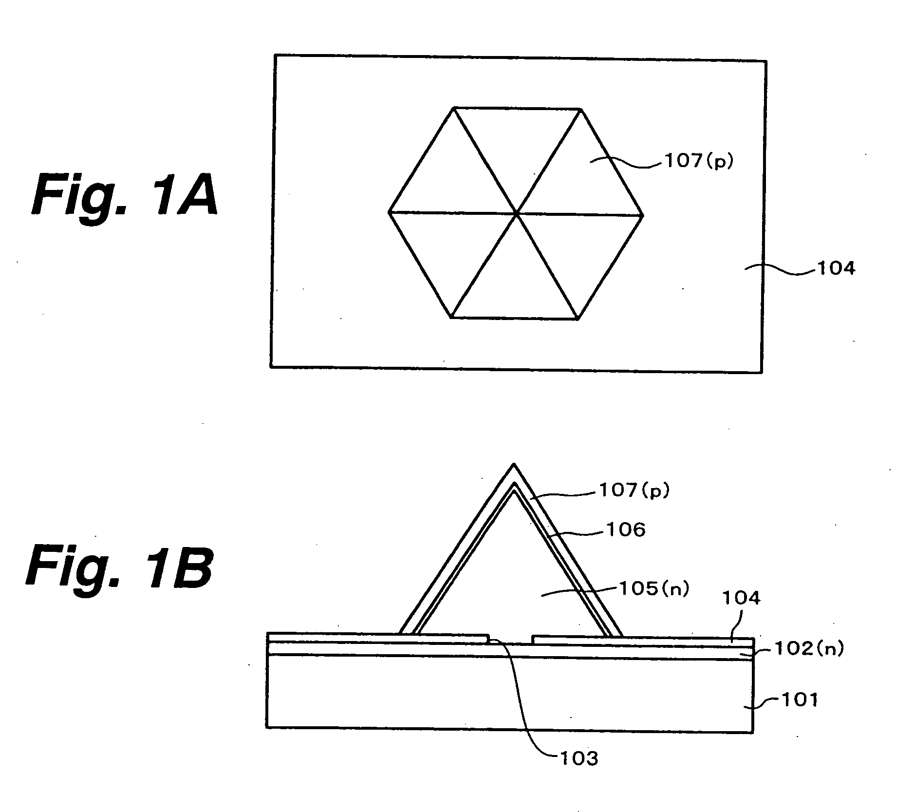
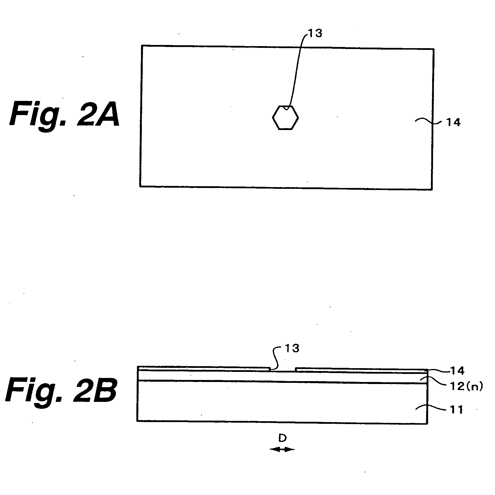
[0126]FIGS. 2A and 2B through FIGS. 5A and 5B show a manufacturing method of a GaN-based light emitting diode according to the invention, in which the figures numbered with the suffix A are plan views whereas the figures numbered with the suffix B are cross-sectional views.

[0127] In the first embodiment, first referring to FIGS. 2A and 2B, a sapphire substrate 11 having a C+oriented major surface, for example, is prepared. After the surface of the sapphire substrate 11 is cleaned by thermal cleaning, for example, an n-type GaN layer 12 doped with an n-type impurity such as Si is grown on the sapphire substrate 11 by metal organic chemical vapor deposition (MOCVD), for example. The n-type GaN layer 12 is desirably minimized in crystal defects and penetrating dislocations, and a thickness around 2 μm will be enough in most cases. Various techniques are employable for forming a defects-reduced n-type GaN layer 12. A typical technique first grows a GaN buffer layer or an AlN buffer laye...

second embodiment

[0149] Next explained is a GaN-based light emitting diode according to the invention.

[0150] In the second embodiment, after the layers are grown up to the p-type GaN layer 17 by the same steps as those of the first embodiment, the p-side electrode 18 is formed on the p-type GaN layer 17. After that, the n-type GaN layer 12 and other upper layers are exfoliated from the sapphire substrate by irradiating a laser beam from the bottom of the sapphire substrate 11 with an excimer laser. Thereafter, the bottom surface of the exfoliated n-type GaN layer 12 is smoothed by etching, for example, and the n-side electrode 19 is formed on the smoothed bottom surface of the n-type GaN layer 12 as shown in FIG. 13. The n-side electrode 19 may be a transparent electrode made of ITO, for example. In this case, the n-side electrode 19 can be formed to lie over the wide area on the bottom surface of the n-type GaN layer 12 including the area under the six-sided steeple-shaped structure. In case the n-...

third embodiment

[0152] Next explained is an image display device according to the invention. FIG. 15 shows the image display device.

[0153] As shown in FIG. 15, the image display device includes GaN-based light emitting diodes regularly aligned in the orthogonal x and y directions in a plane of a sapphire substrate 11 to make a two-dimensional array of GaN-based light emitting diodes. Structure of each GaN-based light emitting diode may be identical to that of the first embodiment, for example.

[0154] In the y direction, GaN-based light emitting diodes for emitting red (R), GaN-based light emitting diodes for emitting green (G) and GaN-based light emitting diodes for emitting blue (B) are aligned in a close relation, and three GaN-based light emitting diodes for different colors compose one pixel. Individual p-side electrodes 18 of GaN-based light emitting diodes for red aligned in the x direction are connected to each other by wiring 22. Similarly, p-side electrodes 18 of the GaN-based light emitti...


PUM

PropertyMeasurementUnit
angleaaaaaaaaaa
sizeaaaaaaaaaa
temperatureaaaaaaaaaa

Abstract

A semiconductor light emitting element, manufacturing method thereof, integrated semiconductor light emitting device, manufacturing method thereof, illuminating device, and manufacturing method thereof are provided. An n-type GaN layer is grown on a sapphire substrate, and a growth mask of SiN, for example, is formed thereon. On the n-type GaN layer exposed through an opening in the growth mask, a six-sided steeple-shaped n-type GaN layer is selectively grown, which has inclined crystal planes each composed of a plurality of crystal planes inclined from the major surface of the sapphire substrate by different angles of inclination to exhibit a convex plane as a whole. On the n-type GaN layer, an active layer and a p-type GaN layer are grown to make a light emitting element structure. Thereafter, a p-side electrode and an n-side electrode are formed.

Description

BACKGROUND OF THE INVENTION [0001] This invention relates to a semiconductor light emitting element, manufacturing thereof, integrated semiconductor light emitting device, manufacturing method thereof, image display device, manufacturing method thereof, illuminating device and manufacturing method thereof, which are especially suitable for application to light emitting diodes using nitride III-V compound semiconductors. [0002] A light emitting diode as a semiconductor light emitting element has been proposed. This semiconductor light emitting element was made by growing an n-type GaN layer on a sapphire substrate; next forming thereon a growth mask having a predetermined opening; selectively growing an n-type GaN layer in form of a six-sided pyramid having an inclined crystal plane inclined from the major surface of the substrate, i.e. having an S-oriented plane; and growing an active layer, p-type GaN layer and other layers on the inclined crystal plane (see, for example, brochure ...

Claims


Application Information

Patent Timeline
Patent Type & Authority Applications(United States)
IPC IPC(8): C23C16/34C02F1/24H01L21/28H01L33/08H01L33/16H01L33/32
CPCH01L21/0237H01L21/02458H01L21/0254H01L21/0262H01L33/32H01L21/02647H01L33/007H01L33/20H01L33/24H01L21/02639H01L2224/48137B01D21/00C02F1/24C02F1/40C02F1/52C02F2201/002C02F2201/46115C02F2209/02C02F2209/40
Inventor OKUYAMA, HIROYUKIDOI, MASATOBIWA, GOSHISUZUKI, JUNOOHATA, TOYOHARU
Owner SONY CORP
Why Eureka
Try Eureka