

Production method of pattern underlay for epitaxial growth of high-crystal quality nitride
A technology of epitaxial growth and crystal quality, applied in semiconductor/solid-state device manufacturing, electrical components, circuits, etc., which can solve the problems of complex process, high cost, and pattern limitation.
- Summary
- Abstract
- Description
- Claims
- Application Information
AI Technical Summary
Problems solved by technology
Method used
Image

Examples
preparation example Construction
[0021] see Figure 1 to Figure 4 , the present invention is a kind of preparation method of pattern substrate used for epitaxial growth of high crystal quality nitride, comprising the following steps:
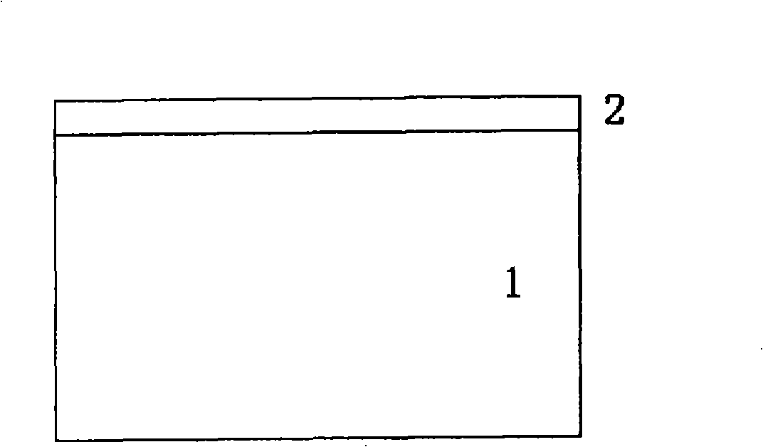
[0022] Step 1: Deposit a thin layer of metal 2 on the substrate 1 (such as figure 1 ); the substrate 1 is a patterned substrate for nitride epitaxial growth; the patterned substrate for nitride epitaxial growth is sapphire, silicon, silicon carbide, gallium arsenide, zinc oxide, self-supporting Any one of gallium nitride; the patterned substrate for nitride epitaxial growth is any one of c-plane (0001), m-plane (1010), r-plane (1102) or a-plane (1120) The effect of the substrate 1 is to etch out the pattern and grow high-quality nitride thereon; the thin metal layer 2 is any one of Ni, Ti, Au or Al; the The thickness of the thin metal layer 2 is 5nm to 30nm; the function of the thin metal layer 2 is to make a mask layer after annealing.
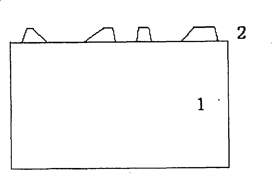
[0023] Step 2: Carry out annealing t...
Embodiment
[0028] This embodiment is a method for fabricating a patterned c-plane or (0001) sapphire substrate for nitride epitaxial growth. The c-plane sapphire substrate is one of the most commonly used substrate materials for epitaxial nitride growth.
[0029] First deposit 15nm metallic nickel (Ni) on a 2-inch c-plane sapphire substrate. figure 1 shown, then at N 2 Under air flow, annealing was carried out at 800°C for 5 minutes. The schematic diagram of the structure section is shown in figure 2 shown;
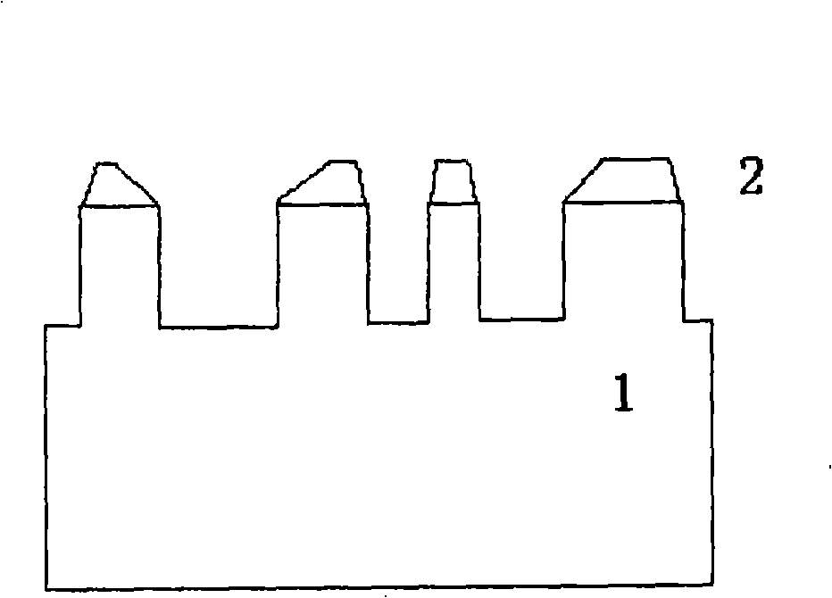
[0030] Then use Ni as a pattern mask, use ICP equipment to dry etch the substrate for 60 seconds, and transfer the mask pattern to the sapphire substrate. The structure profile is as follows image 3 shown;
[0031] Then use hot HNO3 to corrode the substrate for 10 minutes, remove Ni on the sapphire substrate, and clean the sapphire substrate to make a patterned sapphire substrate, the structure profile is as follows Figure 4 shown;
[0032] Figure 5 It is the surface topo...
PUM
| Property | Measurement | Unit |
|---|---|---|
| thickness | aaaaa | aaaaa |
Abstract
Description
Claims
Application Information