Display device and drive method for the same

A technology of a display device and a driving method, which is applied to static indicators, instruments, etc., and can solve problems such as inability to obtain display quality

Inactive Publication Date: 2011-01-19
SHARP KK
View PDF2 Cites 5 Cited by
  • Summary
  • Abstract
  • Description
  • Claims
  • Application Information

AI Technical Summary

Problems solved by technology

As a result, in the case of image display that changes every other frame, good display quality cannot be obtained

Method used


Image

  • Display device and drive method for the same
  • Display device and drive method for the same
  • Display device and drive method for the same

Examples


Embodiment approach 1

[0190]

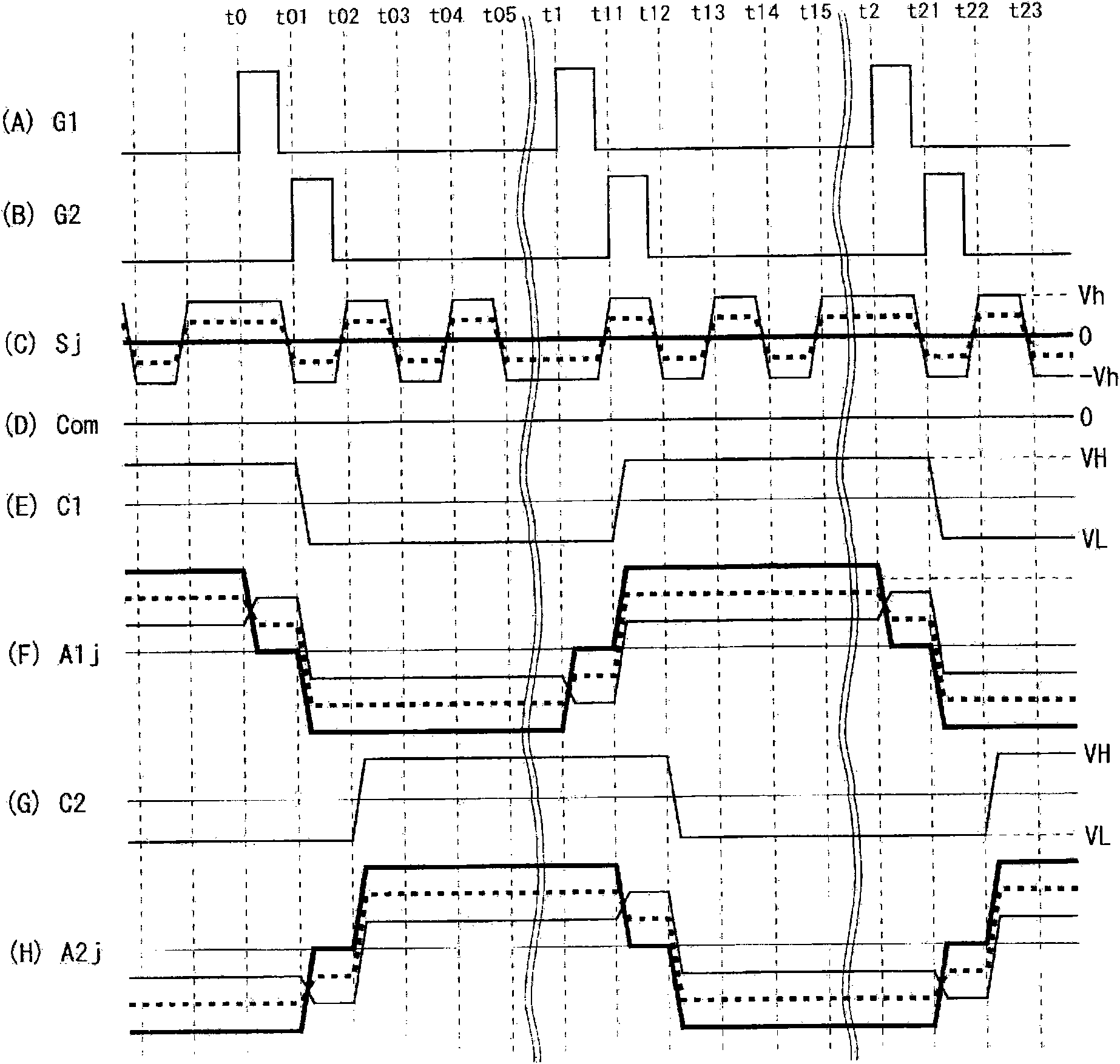
[0191] Image 6 is a liquid crystal display device according to Embodiment 1 of the present invention. A block diagram of the overall structure. The liquid crystal display device includes: a display control circuit 100; a display portion 200; a source driver (video signal line drive circuit) 300; a gate driver (scanning signal line drive circuit) 400; and an auxiliary capacitor driver (an auxiliary capacitor electrode drive circuit) 500. Hereinafter, the source driver 300 , the gate driver 400 , and the auxiliary capacitor driver 500 are collectively referred to as drivers (driver circuits). Figure 7 It is a block diagram showing the detailed configuration of the driver and the display unit 200 in the liquid crystal display device. In addition, a case where 256-gradation grayscale display is performed in this liquid crystal display device will be described.

[0192] The display unit 200 includes: n source wirings (video signal lines) S1 to Sn; m gate wirings (...

Embodiment approach 2

[0272]

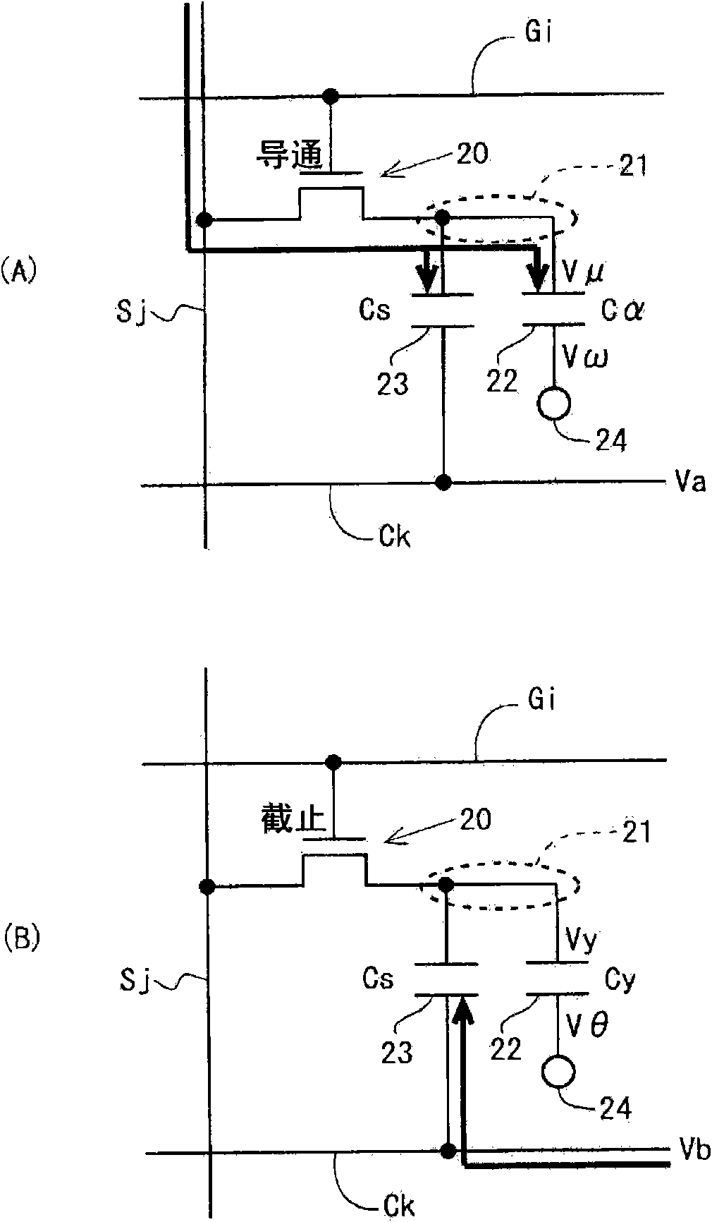
[0273] Figure 10 is a liquid crystal display device according to Embodiment 2 of the present invention. A block diagram of the driver and the detailed structure of the display unit 200 in FIG. In this embodiment, in addition to the constituent elements of Embodiment 1 described above, a counter electrode driver 600 for driving the counter electrode 24 is provided. In addition, the configuration of the source output circuit in the source driver is different from that of Embodiment 1 described above. Other components are the same as those in Embodiment 1, and thus description thereof will be omitted.

[0274] The opposite electrode polarity signal PC from the display control circuit 100 is supplied to the opposite electrode driver 600 . The opposite electrode driver 600 drives the opposite electrode 24 based on the opposite electrode polarity signal. Specifically, the counter electrode driver 600 alternately supplies a voltage of 0 V and the above-mentioned sour...

Embodiment approach 3

[0341]

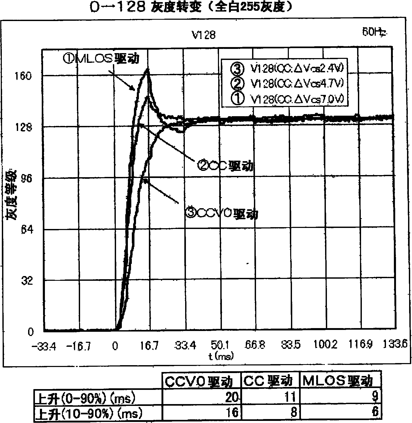
[0342] In the liquid crystal display device of this embodiment, the outline of the configuration of the driver and the display unit 20 is the same as Figure 10 The structure of the above-described second embodiment shown is the same. However, the magnitude of the voltage supplied from the storage capacitor driver 500 to the storage capacitor lines C1 to Cm and the magnitude of the voltage supplied from the counter electrode driver 600 to the counter electrode 24 are different from those of Embodiment 2 described above. Specifically, in Embodiment 2 of the above formula, the counter electrode voltage Vω in the first period is set so as to be equal to the magnitude of the source voltage (the voltage of 0 V or the source high voltage Vh) when the grayscale value is “255”. However, in the present embodiment, the first-period counter electrode voltage Vω is set to "-Vd" on the low potential side and "Vh+Vd" on the high potential side. Therefore, in the present embodime...


PUM


Abstract

There is provided a display device that compensates, without being equipped with a frame memory, change in the capacitance value of an electro-optical element, such as a liquid crystal or the like, occurring with change in the voltage applied to the electro-optical element. The response speed of the display device is also improved. For each of pixel formation portions (A1j, A2j), a frame period is divided into a first period and a second period. In the frame period, a target voltage is applied to the pixel formation portions (A1j, A2j), the target voltage being a voltage having either one of positive and negative polarities relative to the voltage level (Com) of an opposing electrode. In the first period of the frame period, a TFT is brought into a conductive state and a voltage corresponding to the target voltage is applied to a source line (Sj), thereby applying, to a pixel electrode of the pixel formation portions (A1j, A2j), a voltage having the another polarity relative to the voltage level (Com) of the opposing electrode. In the second period of the frame period, the TFT is brought into a non-conductive state and the voltage of an auxiliary capacitor wiring (Ck) is changed from the another polarity to the one polarity relative to the voltage level of the opposing electrode, thereby applying the target voltage to the pixel formation portions (A1j, A2j).

Description

technical field [0001] The present invention relates to a display device such as a liquid crystal display device and a driving method thereof. Background technique [0002] In recent years, liquid crystal display devices using TFT (Thin Film Transistor: Thin Film Transistor), such as notebook computers, mobile phones, and liquid crystal televisions, have become widespread. In a liquid crystal display device using TFTs, in order to control the display state of liquid crystals, a drive circuit called a "source driver" supplies voltage to the liquid crystals. For example, in Japanese Patent Application Laid-Open No. 2002-351409, it is disclosed that Figure 18 The invention of the liquid crystal display device of the structure shown. In this liquid crystal display device, a source driver 907 including a plurality of source driver ICs 908 is provided, and a voltage is supplied from the source driver 907 to the liquid crystal. [0003] Figure 8 It is a circuit diagram showing...

Claims


Application Information

Patent Timeline
Patent Type & Authority Applications(China)
IPC IPC(8): G09G3/36G02F1/133G09G3/20
CPCG09G2320/0252G09G3/3614G09G3/3655G09G2310/08G09G2300/0876
Inventor 沼尾孝次寺沼修
Owner SHARP KK
Why Eureka
Try Eureka