
Method for specific waveform matching in functional test of integrated circuit

A technology for integrated circuit and functional testing, applied in the direction of electronic circuit testing, etc., can solve problems such as high circuit failure rate, inability to perform accurate testing, lack of complete matching of specific waveforms, etc., and achieve the effect of simple and feasible methods

Active Publication Date: 2011-01-26
SINO IC TECH
View PDF6 Cites 6 Cited by
  • Summary
  • Abstract
  • Description
  • Claims
  • Application Information

AI Technical Summary

Problems solved by technology

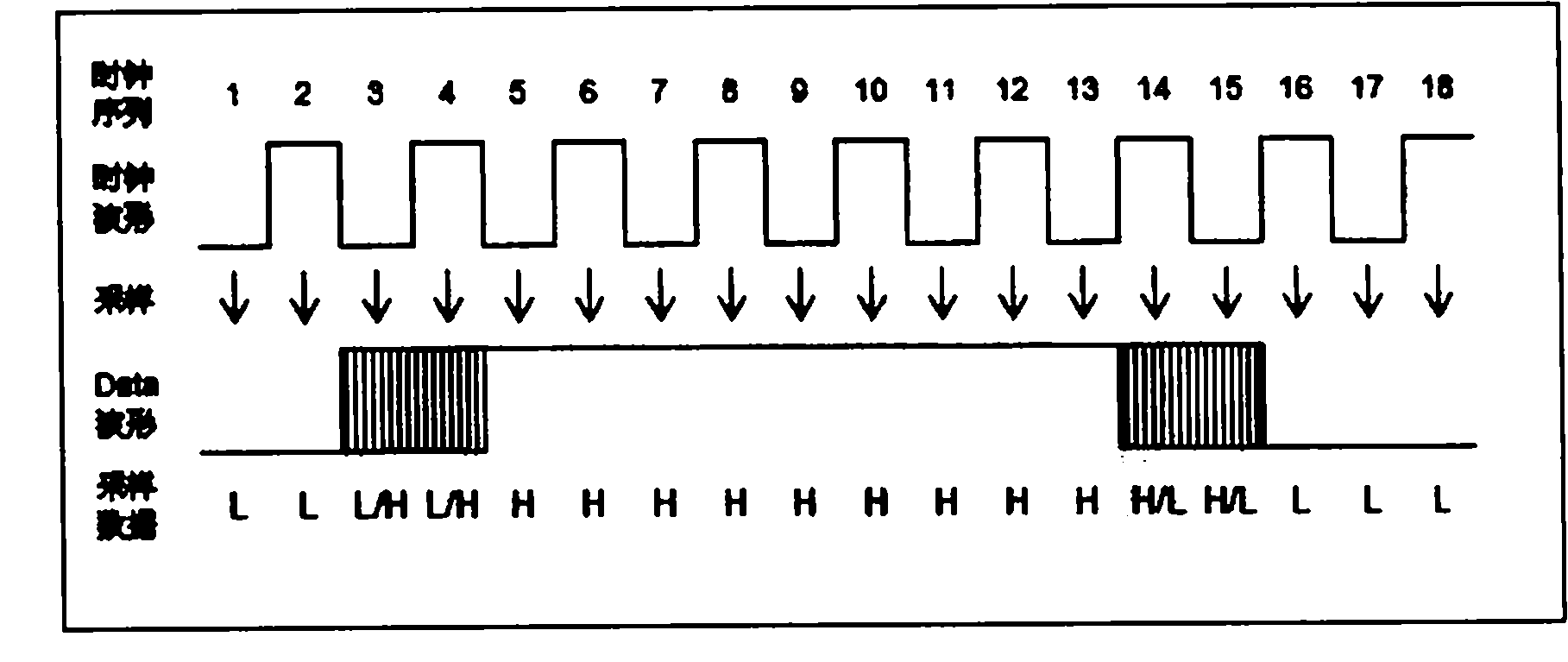
In the currently used integrated circuit test system, only a small number of instructions are configured, and only the edge of a simple level change can be matched. For example, when matching the rising edge of a low-level to high-level change, only the low It can effectively solve the situation of waveform offset and edge uncertainty, but it is powerless when encountering a waveform that needs to match a specific part of the waveform.
In the currently used test circuit / test system, only a small number of instructions are configured to complete simple waveform edge matching, and there is a lack of complete matching of specific waveforms. Therefore, this function cannot be accurately tested, and this functional test can only be abandoned. As a result, the unqualified rate of the circuit in actual use is very high, and users cannot use it

Method used


Image

  • Method for specific waveform matching in functional test of integrated circuit
  • Method for specific waveform matching in functional test of integrated circuit
  • Method for specific waveform matching in functional test of integrated circuit

Examples


Embodiment Construction

[0034] In order to better understand the technical content of the present invention, specific embodiments are given together with the attached drawings for description as follows.

[0035] Below in conjunction with accompanying drawing and specific embodiment the present technical scheme is further described:

[0036] For the implementation process of this technical solution, see Figure 5 , the specific steps are:

[0037] 1. Power on the circuit, apply a specified voltage to the power supply of the circuit, and apply a specified level to the input pin at the same time, so that the circuit enters the working state.

[0038] 2. Perform specific waveform matching.

[0039] 3. Judging whether the matching is completed, if not, continue to match, if it is completed, it means that a specific waveform has been matched, jump out of the matching, enter the function test, and test the output waveform.

[0040] 4. End the test.

[0041] The specific implementation is realized by mo...


PUM


Abstract

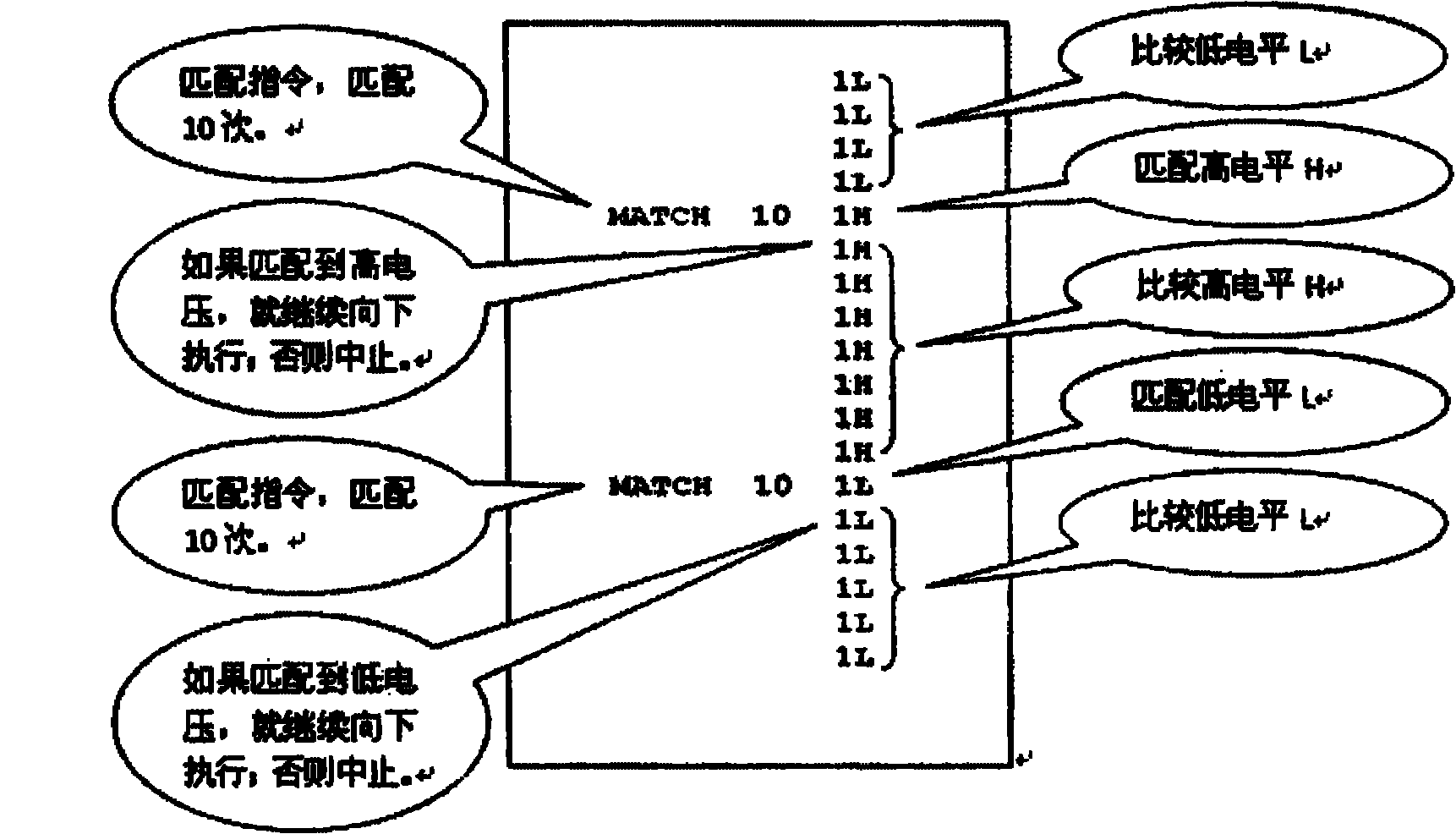
The invention provides a method for specific waveform matching in the functional test of an integrated circuit. During the test of the integrated circuit, the method comprises the following steps of: (1) electrifying a circuit: applying a specified voltage to power pins of the integrated circuit, simultaneously applying a specified level to the input pin so that the integrated circuit enters a working state, and simultaneously acquiring the output level of the Data pin; (2) carrying out specified waveform matching: selecting a part with widest high level in the whole waveform as an initial position, and carrying out matching on the part; (3) judging whether the matching is finished or not, and if the matching is finished, jumping out of matching and entering the functional test, and testing the output waveform; and (4) ending the test. The invention solves the key technical problem of specified waveform matching in output of the integrated circuit and ensures that the function can be accurately tested. By applying the technology and adding the functional test, the passing ratio of the tested circuit is promoted by 20 percent in the actual use.

Description

technical field [0001] The invention belongs to the field of integrated circuit design, in particular to a method for matching specific waveforms in integrated circuit function testing. Background technique [0002] In integrated circuit testing, functional testing is an important part. When performing a functional test, the test system applies an input signal to the input pin of the circuit to put the circuit into a working state, then reads the response signal on the output pin, and the test system samples and compares the signal, which is compared with the stored in the test system. The standard signals are compared, and if they are consistent, it is judged that the function of the circuit is correct, and if they are inconsistent, it is judged that the function of the circuit is abnormal. [0003] There is a prerequisite for using the existing integrated circuit test system for testing: under the same input conditions, the output waveform must also be the same, otherwise...

Claims


Application Information

Patent Timeline
IPC IPC(8): G01R31/28
Inventor 牛勇祁建华徐惠余琨刘远华王锦汤雪飞张志勇叶守银赵达君张映
Owner SINO IC TECH
Learn More