Semiconductor mounting structure and method for manufacturing same

A manufacturing method and semiconductor technology, applied in the direction of semiconductor/solid-state device manufacturing, semiconductor devices, semiconductor/solid-state device components, etc., can solve the problem of resin strength, that is, durability and heat resistance, reduction of heat cycle resistance, environmental pollution, etc. problems, to achieve the effect of improving repairability, easy repair, and improving impact resistance reliability

Inactive Publication Date: 2011-02-02
PANASONIC CORP
View PDF4 Cites 13 Cited by
  • Summary
  • Abstract
  • Description
  • Claims
  • Application Information

AI Technical Summary

Problems solved by technology

[0010] However, for the method disclosed in Patent Document 3, the use of a plasticizer is a necessary condition, and the strength of the resin, that is, the durability, heat resistance, and heat cycle resistance are reduced, and the environment is polluted due to the precipitation of the plasticizer from the cured product. The problem

Method used


Image

  • Semiconductor mounting structure and method for manufacturing same
  • Semiconductor mounting structure and method for manufacturing same
  • Semiconductor mounting structure and method for manufacturing same

Examples


no. 1 Embodiment approach

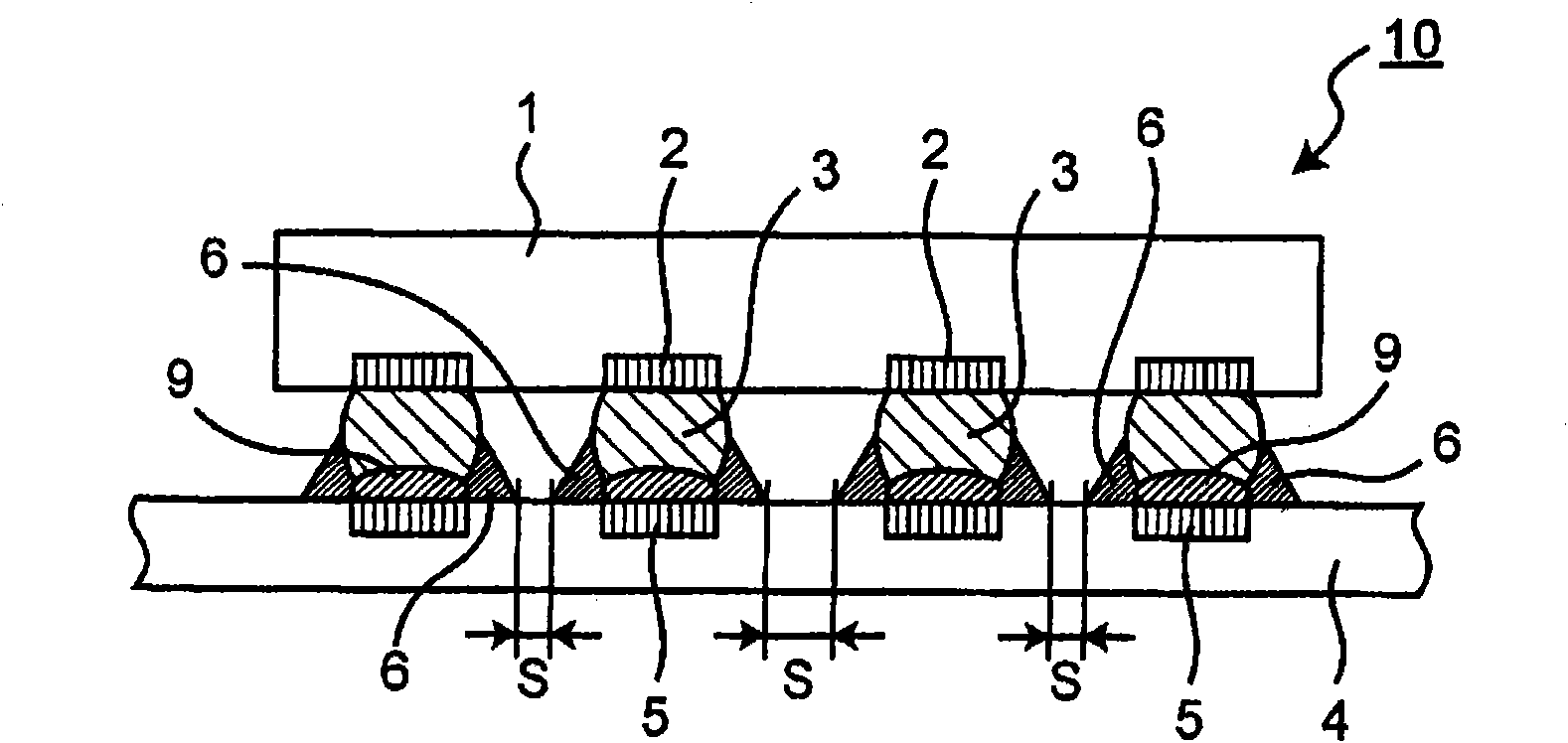
[0038] figure 1 The outline of the mounting structure 10 of the semiconductor package obtained by the mounting method in the first embodiment (an example of a semiconductor includes a case of a semiconductor element alone and a case of a package including a semiconductor element.) 1 Partial sectional view. like figure 1 As shown, the mounting structure 10 includes a BGA semiconductor package 1 having a plurality of electrodes 2 , a solder bump 3 formed on each electrode 2 , and a circuit board 4 having a plurality of substrate electrodes (an example of the second electrode) 5 . , a bonding member 9 that exists between the solder bump 3 and the substrate electrode 5 of the circuit board 4 and electrically connects the solder bump 3 to the substrate electrode 5 , and a reinforcement that is arranged around each bonding member 9 and reinforces the bonding member 9 Resin (reinforced resin member) 6 .

[0039] In the mounting structure 10 of the first embodiment, the solder bump...

no. 2 Embodiment approach

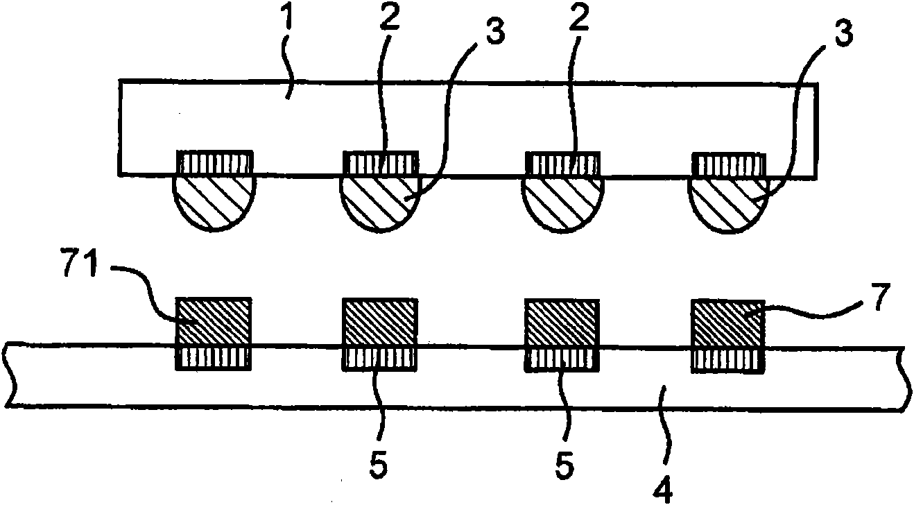
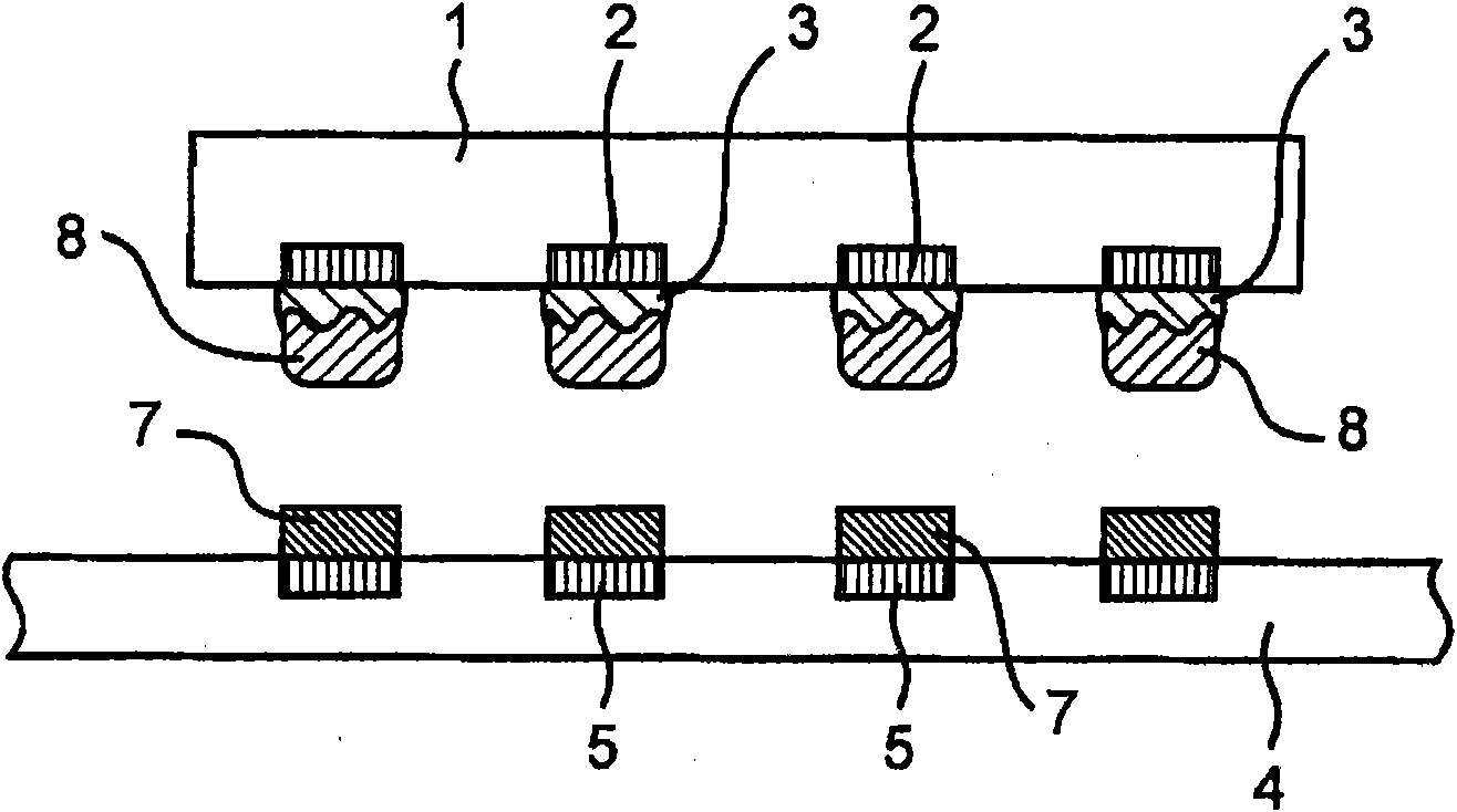
[0053] The second embodiment of the present invention relates to a method of mounting the semiconductor package 1 in one aspect of the present invention, that is, a method of manufacturing the mounting structure 10 of the semiconductor package 1, using figure 2 , image 3 and Figure 4 The mounting methods (manufacturing methods) 1, 2, and 3 of the three patterns will be described. Again, for figure 1 The components of the shown mounting structure 10 that are basically the same are denoted by the same reference numerals, and the description thereof will be omitted.

[0054] (Installation method 1)

[0055] First, the installation method 1 will be described. like figure 2 As shown, a mixed paste 71 (that is, a mixed paste of a solder material and a thermosetting resin) obtained by mixing the following solder material with a thermosetting resin in an uncured state is printed on the substrate electrode 5 of the circuit board 4, so that The solder material is a material co...


PUM


Abstract

A semiconductor mounting structure is provided with: a semiconductor having first electrodes,a circuit board having second electrodes,bumps formed on the first electrodes,bonding members, which are arranged between the bumps and the second electrodes and electrically connect together the first electrodes and the second electrodes with the bumps therebetween,and reinforcing resin members arranged at the periphery of each bonding member so as to cover at least bonding portions between the bumps and the bonding members and the bonding members. The reinforcing resin members are arranged by being spaced apart from each other such that the adjacent reinforcing resin members are not in contact with each other and with the semiconductor. Thus, in the semiconductor mounting structure, impact resistance reliability of connecting sections is improved, and the semiconductor mounting structure can be easily repaired.

Description

technical field [0001] The present invention relates to a semiconductor mounting structure in which semiconductors such as a semiconductor chip (semiconductor element) and a semiconductor package are electrically connected to a circuit board, and a method for manufacturing the same. Background technique [0002] Mobile devices such as mobile phones and PDAs (Personal Digital Assistants) are becoming smaller and more functional, and mounting structures such as BGA (Ball Grid Array) and CSP (Chip Scale Package) are widely used as mounting technologies that can cope with this. . Mobile equipment is susceptible to mechanical loads such as drop shocks. Therefore, for mounting structures such as BGAs and CSPs that do not have shock-mitigating mechanisms, such as lead wires of a QFP (Quad Flat Package), it is important to secure shock-resistant reliability of the solder connection. [0003] Therefore, for example, when connecting a BGA type semiconductor package and an electronic...

Claims


Application Information

Patent Timeline
Patent Type & Authority Applications(China)
IPC IPC(8): H01L21/60
CPCH01L2224/73203H05K2201/10992H01L2924/01082H01L2924/01004H01L2924/01049H01L2224/81801H01L2224/13109H05K3/3463H01L2924/01029H01L24/12H01L2224/13099H01L2224/83192H01L2924/01027H01L21/563H01L2924/014H01L2924/01013H01L2224/10126H05K3/3484H01L2924/0103H01L2224/83855H01L2224/83194H01L2924/01047H01L23/49816H01L2924/01079H01L24/81H01L24/16H01L2924/01033H01L2924/01006H05K3/3452H01L23/49894H01L2224/131H05K2201/10977H01L2924/01075H01L2224/83856H01L2224/16225H05K3/3436H01L2224/13566H01L2224/812H01L2224/16058H01L2224/13111H05K3/3485Y02P70/50H01L2924/01083H01L2924/00014H01L2924/0105
Inventor 大桥直伦酒谷茂昭岸新山口敦史宫川秀规
Owner PANASONIC CORP
Why Eureka
Try Eureka