Gold-plating method of long and short golden fingers

A gold-plated area and manufacturing process technology, applied in the direction of electrical connection of printed components, printed circuit components, conductive pattern formation, etc., can solve the problems of difficult control of key dimensions of gold fingers, long time spent on gold-plated wires, poor graphics and dimensional accuracy, etc. , to achieve the effect of shortening the production cycle, flexible production arrangement and less process

Inactive Publication Date: 2012-07-04
SHENNAN CIRCUITS
View PDF0 Cites 0 Cited by
  • Summary
  • Abstract
  • Description
  • Claims
  • Application Information

AI Technical Summary

Problems solved by technology

[0005] The production cycle is long, because the process of protecting and removing gold-plated wires takes a long time, it usually takes 2-4 days to deal with such processes; the cost is high;
[0006] (2) The root of the gold finger is prone to recessed corrosion. Because the gold-plated area and the gold-plated wire are connected to each other, after the gold-plated wire is etched away, part of the copper layer under the nickel-gold layer connected to the gold finger and the wire is easily etched away, resulting in recessed etching. It is easy to fail in the salt spray test;
[0007] (3) It is difficult to control the key dimensions of the gold finger: it needs to go through two graphics transfers, the first time is the outer picture when making the in-board graphics and gold finger graphics, and the second is the solder mask when protecting the gold-plated wire. Dimensional accuracy is poor

Method used


Image

  • Gold-plating method of long and short golden fingers
  • Gold-plating method of long and short golden fingers
  • Gold-plating method of long and short golden fingers

Examples


Embodiment 1

[0031] Embodiment 1 of the gold-plating method as the long and short golden fingers of the present invention includes:

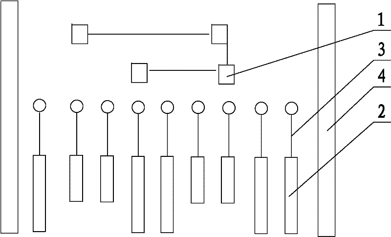
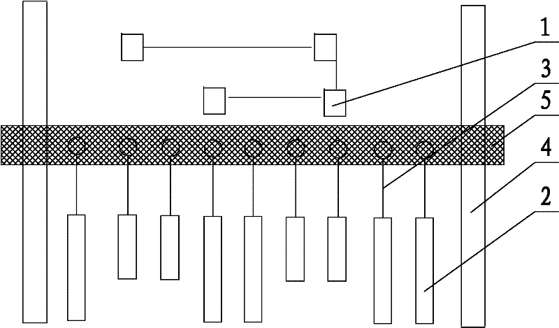
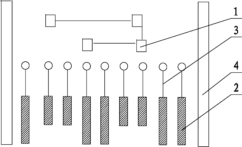
[0032] (1) Prepare the PCB board, and make the in-board graphic 1 and the long and short gold finger 2 graphics on the PCB. The long and short gold fingers 2 are connected to the on-board graphic 1 through the lead wire 3, and all the lead wires 3 form a connection area;

[0033] (2) Screen printing conductive ink 5, the conductive ink 5 in the screen printing area covers the connection area between the long and short golden fingers 2 and the graphics 1 on the board, so that all the leads 3 are electrically connected to each other. In order to save time, it is generally necessary to complete the screen printing. The conductive ink is dried, the baking temperature is 120°C, and the baking time is 30 minutes;

[0034] (3) Utilize the conductive ink 5 as the gold-plated wire to carry out gold-plating to the long and short gold fingers 2;

[0035] (4) Remove th...


PUM


Abstract

The invention relates to a gold-plating method of long and short golden fingers, comprising: (1) preparing a printed circuit board (PCB) board, manufacturing a pattern in a board and long and short golden finger patterns on the PCB board, causing the long and short golden fingers to mutually conduct with the pattern in the board by leads, and forming a connection area on the junction of all leads; (2) carrying out screen printing of conductive ink, covering the connection area of the long and short golden fingers and the pattern in the board by the conductive ink in a screen printing area, and mutually and electrically conducting all the leads; (3) taking the conductive ink as a gold-plating wire to plate gold on the long and short golden fingers; and (4) removing the conductive ink. Compared with the prior art, the invention has the advantages that the PCB board is not provided with the gold-plating wire, thus flows of manufacturing the gold-plating wires, protecting the gold-platingwires, finally removing the gold-plating wires and the like are naturally omitted; and in addition, the printed conductive ink is adopted to replace the gold-plating wire so as to achieve the purposeof mutually conducting the long and short golden fingers, and the method provided by the invention has the advantages of less flows, short production period, low cost and the like.

Description

technical field [0001] The invention relates to a gold plating method for long and short gold fingers. Background technique [0002] Some PCB boards will have long and short gold fingers due to the need for the interface. In the process of making gold fingers and gold-plating the gold fingers, the method adopted in the prior art is to first etch the gold fingers and graphics on the PCB board and make gold-plated wires. The gold-plated wires make the gold fingers conduction with each other, and then print a wet film on the PCB board and solidify it to protect the gold-plated wires from being plated with nickel gold, and then gold-plate the long and short gold fingers, and then use acid etching to remove the gold-plated wires. The gold plated wires are etched away. The above-mentioned gold-plated wire is actually a process auxiliary wire, which is not retained in the final product. [0003] The production method of the prior art long and short golden fingers has the followin...

Claims


Application Information

Patent Timeline
Patent Type & Authority Patents(China)
IPC IPC(8): H05K3/12H05K1/11
Inventor 刘宝林蒋卓康罗斌
Owner SHENNAN CIRCUITS
Why Eureka
Try Eureka