Process for plating gold on long and short gold fingers

A gold finger, length and short technology, which is applied in the field of gold plating process of long and short gold fingers, can solve the problems of difficult control of key dimensions of gold fingers, long time spent on gold-plated wires, poor graphics and dimensional accuracy, etc., so as to shorten the production cycle and flexibly arrange production. , the effect of less process

Inactive Publication Date: 2013-01-23
SHENNAN CIRCUITS
View PDF2 Cites 0 Cited by
  • Summary
  • Abstract
  • Description
  • Claims
  • Application Information

AI Technical Summary

Problems solved by technology

[0005] The production cycle is long, because the process of protecting and removing gold-plated wires takes a long time, it usually takes 2-4 days to deal with such processes; the cost is high;
[0006] (2) The root of the gold finger is prone to recessed corrosion. Because the gold-plated area and the gold-plated wire are connected to each other, after the gold-plated wire is etched away, part of the copper layer under the nickel-gold layer connected to the gold finger and the wire is easily etched away, resulting in recessed etching. It is easy to fail in the salt spray test;
[0007] (3) It is difficult to control the key dimensions of the gold finger: two graphics transfers are required. The first time is to make the on-board graphics through the external picture, including the gold finger and the gold-plated wire, and the second time is to protect the gold-plated wire from being plated with nickel gold. Conducted solder mask with poor graphic and dimensional accuracy

Method used


Image

  • Process for plating gold on long and short gold fingers
  • Process for plating gold on long and short gold fingers
  • Process for plating gold on long and short gold fingers

Examples


Embodiment Construction

[0031] In order to describe the technical content, structural features, achieved goals and effects of the present invention in detail, the following will be described in detail in conjunction with the embodiments and accompanying drawings.

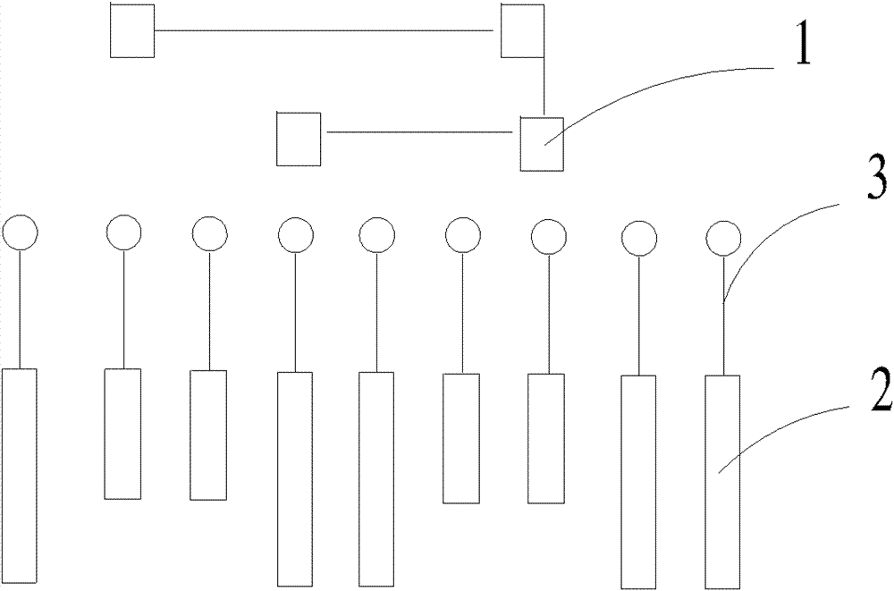
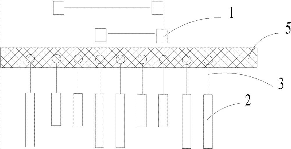
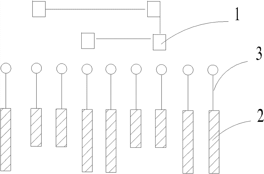
[0032] see Figure 1-Figure 3 , the gold plating process of the long and short golden fingers 2 of the first embodiment of the present invention comprises the following steps:

[0033] Prepare a PCB board, and make an in-board graphic 1 and a long and short gold finger 2 on the PCB, and the long and short gold fingers 2 are connected to the in-board graphic 1 through the lead 3;

[0034] Use conductive tape 5 to stick the lead wires 3 of the long and short gold fingers 2 in sequence, so that the long and short gold fingers 2 are connected to each other;

[0035] Utilize the conductive tape 5 as the gold-plated wire to carry out gold-plating to the long and short gold fingers 2;

[0036] Tear off the conductive tape 5 .

[0037] Compared...


PUM


Abstract

The invention discloses a process for plating gold on long and short gold fingers. The process comprises the following steps of: preparing a printed circuit board (PCB), making an inboard pattern and long and short gold finger patterns on the PCB and conducting the long and short gold fingers with the inboard pattern through leads; sticking the leads of the long and short gold fingers in turn by using conductive tapes and conducting the long and short gold fingers with each other; plating gold on the long and short gold fingers by taking the conductive tapes as gold-plating leads; and tearingthe conductive tapes off. Compared with the prior art, the process does not arrange any gold-plating lead on the PCB and naturally reduces flows for making the gold-plating lead, protecting the gold-plating lead, removing the gold-plating lead and the like. Moreover, the gold-plating lead is replaced by sticking the conductive tape, so that the aim of conducting the long and short gold fingers isfulfilled. The process has the advantages of a small number of flows, short production period, low cost and the like.

Description

technical field [0001] The invention relates to a circuit board processing technology, in particular to a gold plating process for long and short gold fingers. Background technique [0002] Some PCB boards will have long and short gold fingers due to the need for the interface. In the process of making gold fingers and gold-plating the gold fingers, the method adopted in the prior art is to first etch the gold fingers and graphics on the PCB board and make gold-plated wires. The gold-plated wires make the gold fingers conduction with each other, and then print a wet film on the PCB board and solidify it to protect the gold-plated wires from being plated with nickel gold, and then gold-plate the long and short gold fingers, and then use acid etching to remove the gold-plated wires. The gold plated wires are etched away. The above-mentioned gold-plated wire is actually a process auxiliary wire, which is not retained in the final product. [0003] The production method of the...

Claims


Application Information

Patent Timeline
Patent Type & Authority Patents(China)
IPC IPC(8): H05K3/40H05K3/18
Inventor 刘宝林蒋卓康罗斌
Owner SHENNAN CIRCUITS
Why Eureka
Try Eureka