Voltage regulator
A voltage regulator, voltage technology, applied in the direction of regulating electrical variables, control/regulating systems, instruments, etc., can solve the problems of no standby operation, no reverse current flow of Pch transistors, etc., to achieve the effect of low current consumption
- Summary
- Abstract
- Description
- Claims
- Application Information
AI Technical Summary
Problems solved by technology
Method used
Image

Examples
Embodiment 1
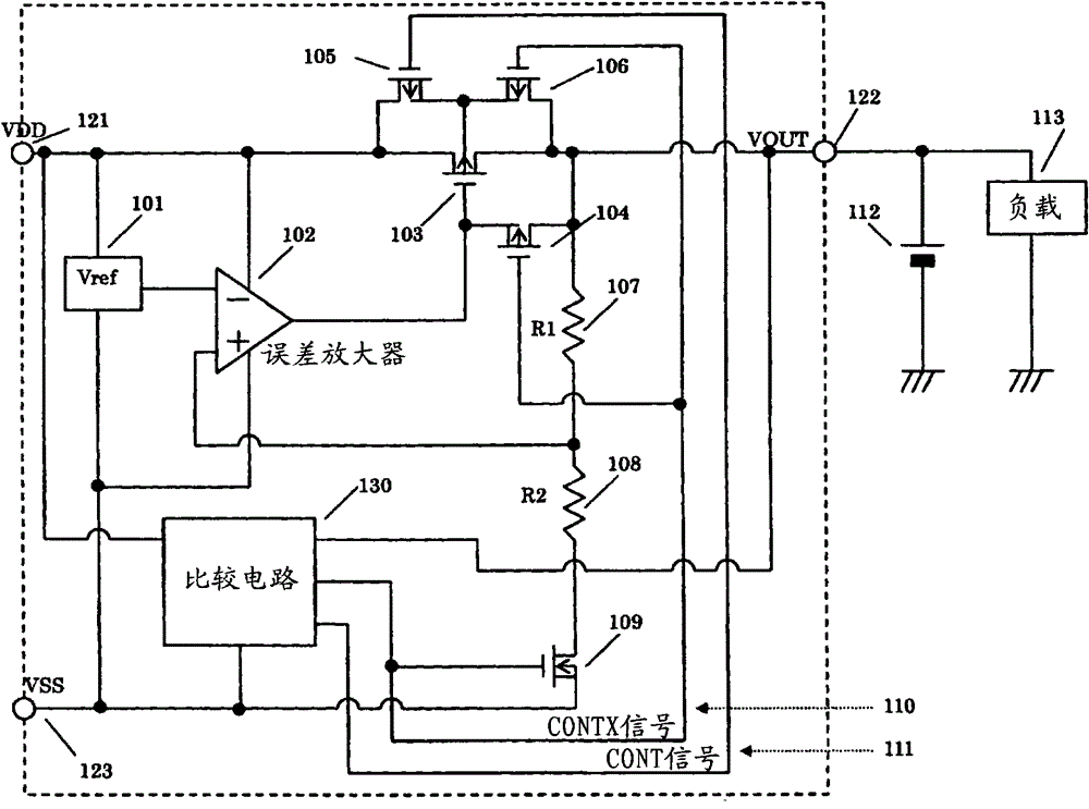
[0032] figure 1 is a circuit diagram showing the voltage regulator of the first embodiment of the present invention. The voltage regulator of the present invention is composed of the following parts: Vref circuit 101, error amplifier 102, comparison circuit 130, resistor 107, resistor 108, Pch (P channel) transistor 103, Pch transistor 104, Pch transistor 105, Pch transistor 106, Nch (N channel) transistor 109 , VDD terminal 121 , VSS terminal 123 , and output terminal 122 . and Figure 11 The difference is that the comparator 1105 and the resistors 1101 , 1102 , 1103 , and 1104 are deleted, and the comparison circuit 130 is used to control the Pch transistors 105 , 106 and the added Pch transistor 104 .
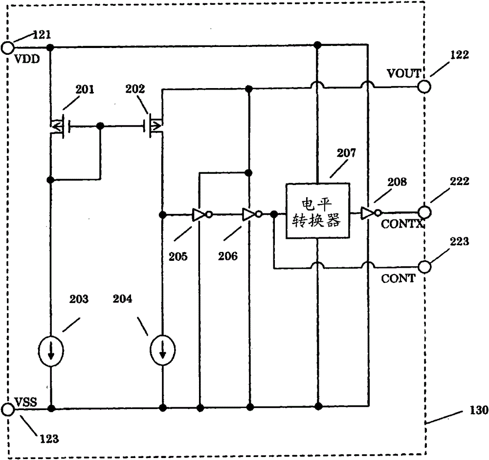
[0033] figure 2 The comparison circuit of the present invention is shown.
[0034] The comparison circuit 130 is composed of the following parts: a constant current circuit 203 , a constant current circuit 204 , a Pch transistor 201 , a Pch transistor 202 , an inverter ...
Embodiment 2
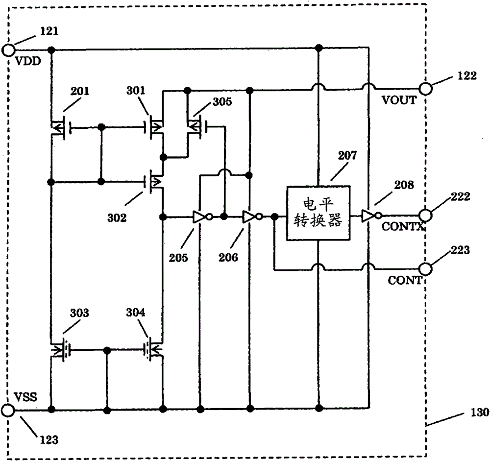
[0047] image 3 show figure 1 The second embodiment of the comparison circuit 130 of the voltage regulator of the present invention. The comparison circuit 130 of the second embodiment is composed of the following parts: constant current circuit 303, constant current circuit 304, Pch transistor 201, Pch transistor 301, Pch transistor 302, Pch transistor 305, inverter 205, inverter 206, inverter A phaser 208 and a level shifter 207 are formed. and figure 2 The difference is that the portion corresponding to the Pch transistor 202 is composed of two transistors, the Pch transistor 301 and the Pch transistor 302, and a Pch transistor 305 for realizing the hysteresis function is added. In addition, the constant current circuit 203 and the constant current circuit 204 are specifically represented by N-channel depletion type MOS transistors whose gates and sources are connected to the VSS terminal 123 .
[0048]Next, the connection of the comparison circuit 130 will be describ...
Embodiment 3
[0060] Figure 5 show figure 1 The third embodiment of the comparison circuit 130 of the voltage regulator of the present invention. The comparison circuit 130 of the third embodiment is composed of the following parts: constant current circuit 303, constant current circuit 304, Pch transistor 202, Pch transistor 501, Pch transistor 502, Pch transistor 503, inverter 205, inverter 206, inverter Phaser 208 and level shifter 207. and figure 2 The difference is that the portion corresponding to the Pch transistor 201 is composed of two transistors, a Pch transistor 501 and a Pch transistor 502, and a Pch transistor 503 for realizing a hysteresis function is added. Additionally, with image 3 Similarly, the constant current circuit 203 and the constant current circuit 204 are specifically represented by N-channel depletion MOS transistors whose gates and sources are connected to the VSS terminal 123 .
[0061] Next, the connection of the comparison circuit 130 will be descri...
PUM
 Abstract
Description
Claims
Application Information
 - R&D Engineer
- R&D Manager
- IP Professional
- Industry Leading Data Capabilities
- Powerful AI technology
- Patent DNA Extraction
Browse by: Latest US Patents, China's latest patents, Technical Efficacy Thesaurus, Application Domain, Technology Topic.
© 2024 PatSnap. All rights reserved.Legal|Privacy policy|Modern Slavery Act Transparency Statement|Sitemap