Time-delay circuit for high-voltage integrated circuit
A high-voltage integrated circuit and delay circuit technology, applied in electrical components, single output arrangement, pulse processing, etc., can solve the problems of non-reset, malfunction of high-voltage integrated circuits, high level, etc., to achieve the effect of improving reliability
- Summary
- Abstract
- Description
- Claims
- Application Information
AI Technical Summary
Problems solved by technology
Method used
Image
Examples
Embodiment Construction
[0040] The content of the present invention will be further described below in conjunction with the accompanying drawings.
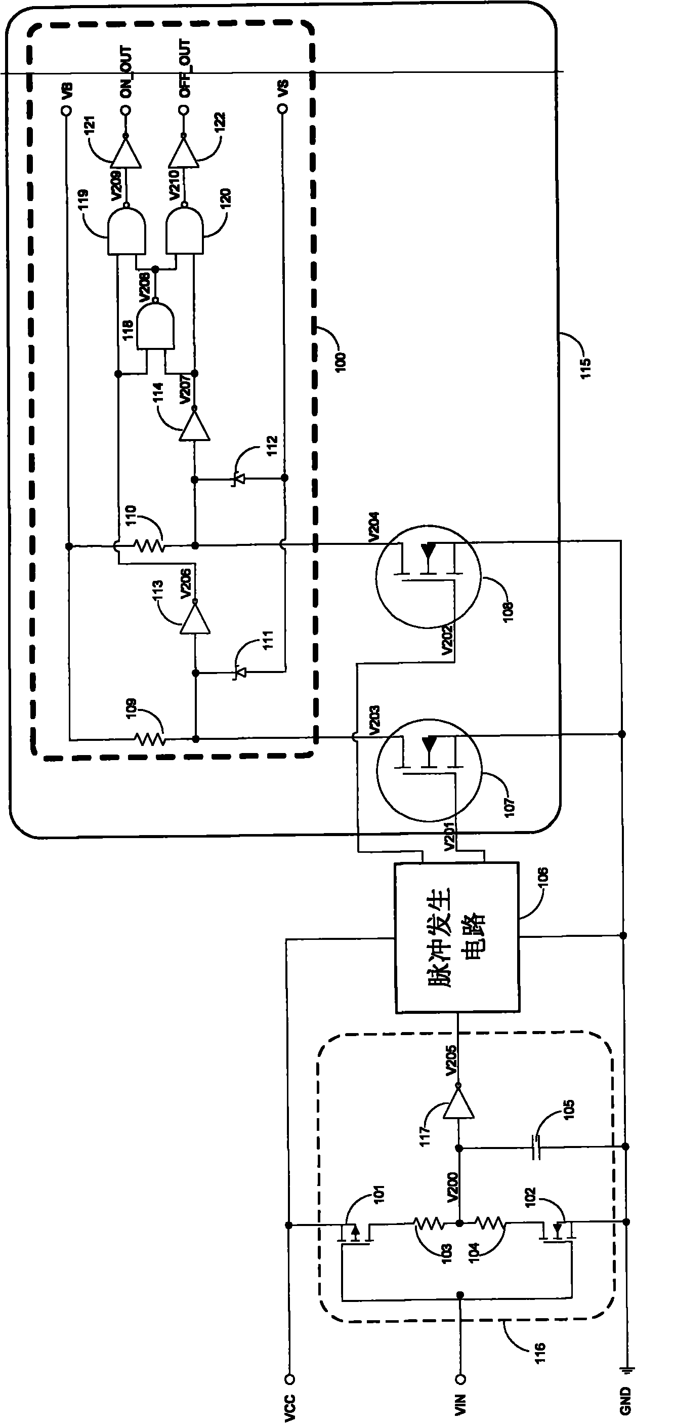
[0041] figure 1 Structural diagram of a traditional delay circuit in a high-voltage integrated circuit. Such as figure 1 As shown, the delay circuit structure diagram currently used in high-voltage integrated circuits, in order to facilitate the description of the working principle of high-voltage integrated circuit signals from low-voltage areas to high-voltage areas, figure 1 Also included in the follow-up pulse generation circuit and level conversion circuit.
[0042]The delay circuit 116 is powered by a low voltage side power supply (VCC-GND), the input signal VIN is connected to the gates of the first PMOS transistor 101 and the first NMOS transistor 102, and the source of the first PMOS transistor 101 is connected to the substrate and connected to VCC, the source of the first NMOS transistor 102 is connected to the substrate and connected to GND...
PUM
 Abstract
Description
Claims
Application Information


