Pulse density modulator for time division-synchronization code division multiple access (TD-SCDMA) and 4G terminal

A TD-SCDMA and pulse density modulation technology, which is applied in the field of pulse density modulators, can solve the problems of slow filter response speed and long modulation period, etc.

Inactive Publication Date: 2013-01-16
ZHEJIANG HUALI COMM TECH
View PDF0 Cites 0 Cited by
  • Summary
  • Abstract
  • Description
  • Claims
  • Application Information

AI Technical Summary

Problems solved by technology

For example, when the number of digits of the digital signal to be modulated increases, the modulation period becomes longer accordingly, and the response speed of the filter becomes slower accordingly.

Method used


Image

  • Pulse density modulator for time division-synchronization code division multiple access (TD-SCDMA) and 4G terminal
  • Pulse density modulator for time division-synchronization code division multiple access (TD-SCDMA) and 4G terminal
  • Pulse density modulator for time division-synchronization code division multiple access (TD-SCDMA) and 4G terminal

Examples


Embodiment 1

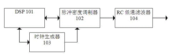
[0080] Example 1: figure 1 It is a block diagram of the pulse density modulation system proposed in this design for TD-SCDMA, Beyond 3G, and 4G terminals. The pulse density modulation system consists of the following components:

[0081] (1) Controller with DSP as the core (No. 101)

[0082] (2) Pulse Density Modulator PDM (102)

[0083] (3) Clock generator (103)

[0084] (4) Pulse density modulator off-chip RC low-pass filter (104)

[0085] Wherein, the DSP 101 provides a control signal for the pulse density modulator PDM 102 to control the level amplitude of the output signal of the pulse density modulator PDM 102 and the refresh rate of the output signal. The clock generator 103 provides a working clock signal for the pulse density modulator PDM 102 . An off-chip RC low pass filter 104 is then used to convert the output of the pulse density modulator PDM 102 into an analog signal.

[0086] In the above-mentioned pulse density modulation system, the pulse density modul...

Embodiment 2

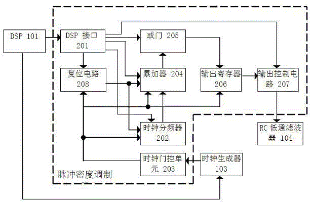
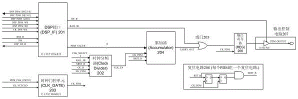
[0104] Embodiment 2: The relationship between PDM102 and the external and internal detailed input and output signals, such as image 3 shown.

[0105] The input and output signals of the DSP interface 201 are shown in Table 1.

[0106] The input and output signals of the clock gating unit 203 are shown in Table 2.

[0107] The input and output signals of the accumulator 204 are shown in Table 3.

[0108] The input and output signals of the clock divider 202 are shown in Table 4.

[0109] The input and output signals of the OR gate 205 are shown in Table 5.

[0110] The input and output signals of the output control circuit 207 are shown in Table 7.

[0111] The input and output signals of the reset circuit 208 are shown in Table 8.

Embodiment 3

[0112] Embodiment 3: PDM 102 outputs logic 1 and logic 0. Its output is passed through an analog low-pass off-chip filter to generate an analog value. When it outputs a high-level signal, the voltage is very close to the power supply voltage Vcc (3.3V in this design), and when it outputs a low-level signal, the voltage is very close to the ground GND voltage.

[0113] PDM 102 should have sufficient resolution to perform the above tasks. Currently, we expect 12-bit resolution. Also, the PDM 102 can output from V L to V H (where V L is the voltage corresponding to a logic low level, V H is the voltage corresponding to the logic high level) all voltage values ​​​​in the range. At the same time, the output of the PDM 102 can also be set to a high-impedance state Hi-Z (ie, the PDM output is set to output prohibition. Output prohibition is only performed on the output pin).

[0114] The refresh rate of PDM 102 can be set by DSP 101 using DSP software / firmware, with faster r...


PUM


Abstract

The invention provides a pulse density modulator for a time division-synchronization code division multiple access (TD-SCDMA) and fourth generation (4G) terminal. When the modulator outputs a high level signal, the voltage is close to power supply voltage Vcc, while when the modulator outputs a low level signal, the voltage is close to ground GND voltage. The pulse density modulator (PDM) has multi-bit represented high resolution ratio, and can output all voltage values in a range from a logical low level to a logical high level. The output of the PDM can be set to be in a high impedance state. The refresh rate of the PDM can be set by a digital signal processor (DSP) in DSP software / firmware. When a plurality of PDMs are used simultaneously, all the PDMs can be divided into a plurality of groups, wherein, each group of PDMs can enable independently, and the groups are controlled by an enable signal of a PDM clock. The PDM is reset when receiving a reset signal of the DSP, and is initialized to be in the high impedance state.

Description

technical field [0001] The invention proposes a pulse density modulator for TD-SCDMA, B3G (Beyond 3G), 4G (fourth generation mobile communication) terminals, which belongs to the field of mobile communication technology manufacturing. Background technique [0002] In digital signal processing, it is often necessary to convert multi-bit digital signals into one-bit digital signals. For example, in the field of communication, the receiver needs to convert the encoded digital voice signal into an analog signal, that is, restore the original analog voice signal. Coded speech signal, usually a multi-bit bit stream. Therefore, how to convert multi-bit bit streams into analog voice signals has become the key to ensuring communication quality. As another example, in some control circuits, the control signal is a multi-bit digital signal generated by calculation, and these digital signals must be converted into analog signals to control the circuit. Therefore, how to convert multi...

Claims


Application Information

Patent Timeline
Patent Type & Authority Patents(China)
IPC IPC(8): H03K7/08H03M1/82
Inventor 许晓斌许雪琦
Owner ZHEJIANG HUALI COMM TECH
Why Eureka
Try Eureka