Method for etching silicon wafer
A technology of silicon wafer and etching gas, which is applied in the manufacture of electrical components, semiconductor/solid-state devices, circuits, etc., can solve the problems of increasing the power maintenance time of the upper and lower electrodes, limited effect, and affecting the etching result, so as to avoid etching The effect of defects
- Summary
- Abstract
- Description
- Claims
- Application Information
AI Technical Summary
Problems solved by technology
Method used
Image

Examples
Embodiment
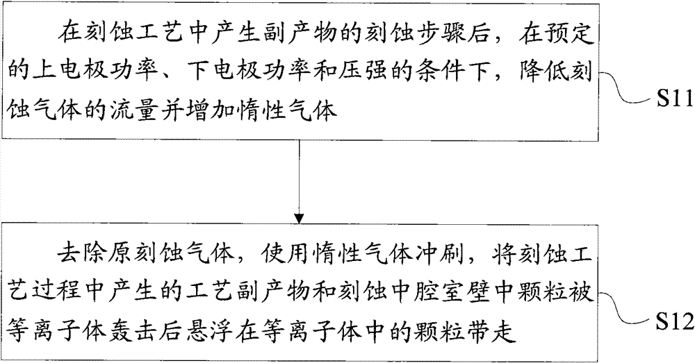
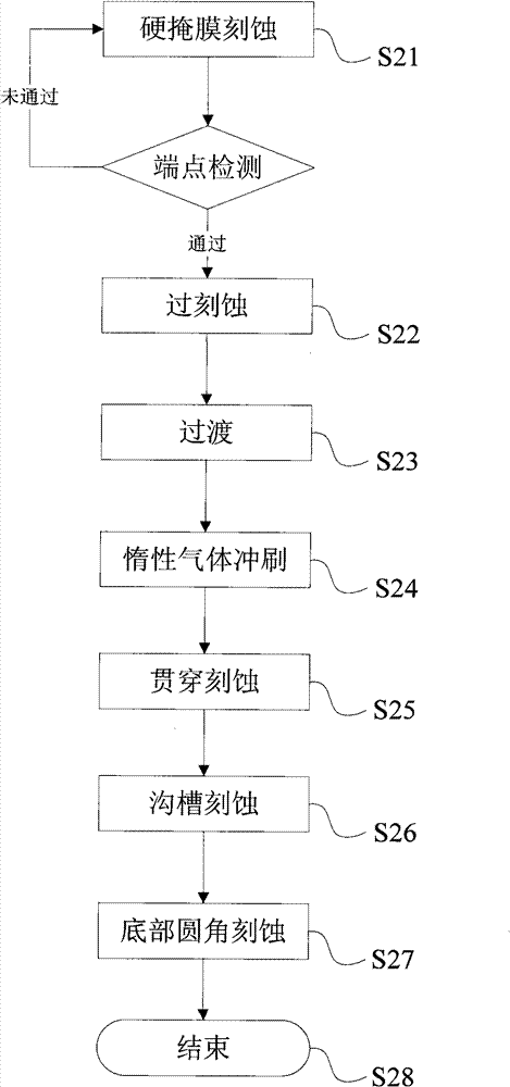
[0025] This embodiment is an STI process applying the etching method of the present invention. figure 2 It is the process flow chart of this embodiment. Such as figure 2 As shown, this embodiment includes the following steps:
[0026] S21, hard mask etching, etching SiNx. The condition parameters are: pressure 8mT; upper electrode power 600W, lower electrode power 90W; etching gas is CF 4 and CH 2 f 2 , the flow rate is 15 sccm; this step is to perform endpoint detection to judge whether the etching step is completed, and if the detection is passed, proceed to the next step.
[0027] S22, over etching, etching, high selectivity etching to remove polysilicon. The condition parameters are: pressure 15mT; upper electrode power 450W, lower electrode power 100W; etching gas is CF 4 and CH 2 f 2 , the flow rate is 30sccm; the duration is 20S.
[0028] S23. Transition step. Since in the two etching steps of S21 and S22, the etching gas used includes CH 2 f 2 , easy to ...
PUM
 Abstract
Description
Claims
Application Information
 - Generate Ideas
- Intellectual Property
- Life Sciences
- Materials
- Tech Scout
- Unparalleled Data Quality
- Higher Quality Content
- 60% Fewer Hallucinations
Browse by: Latest US Patents, China's latest patents, Technical Efficacy Thesaurus, Application Domain, Technology Topic, Popular Technical Reports.
© 2025 PatSnap. All rights reserved.Legal|Privacy policy|Modern Slavery Act Transparency Statement|Sitemap|About US| Contact US: help@patsnap.com