Method for Fabricating A Semiconductor Device Comprising Surface Cleaning

a surface cleaning and semiconductor technology, applied in semiconductor/solid-state device manufacturing, basic electric elements, electric devices, etc., can solve the problems of reducing the design rule, restricting the removal of surface contaminants, and limiting the process margin, so as to prevent corrosion loss and efficiently remove native oxides

Inactive Publication Date: 2008-02-21
SK HYNIX INC
View PDF11 Cites 260 Cited by
  • Summary
  • Abstract
  • Description
  • Claims
  • Application Information

AI Technical Summary

Benefits of technology

[0022]The invention provides a method for fabricating a semiconductor device including surface cleaning capable of efficiently removing a native oxide while preventing the corrosion loss of interlayer dielectric layers.

Problems solved by technology

In addition, the reduction in the design rule has introduced limitations in the process margin as well as restrictions on the removal of surface contaminants (e.g., native oxides) during the formation of connection wiring structures or devices.
During wet cleaning, there occurs undesirable corrosion loss of an insulating layer constituting the sidewalls of contact holes.
The corrosion loss is a restriction or limiting factor of wet cleaning.
More specifically, the reduction in the design rule for semiconductor devices causes a small-sized linewidth of an insulating layer for isolating adjacent contact holes from each other.
Accordingly, the loss of the insulating layer during conventional wet cleaning makes it difficult to secure a predetermined space between adjacent contact holes.
As a result, an electric short circuit between connection contacts filling the contact holes may occur.
In addition, a leakage current in transistors connected to the connection contacts may occur.

Method used


Image

  • Method for Fabricating A Semiconductor Device Comprising Surface Cleaning
  • Method for Fabricating A Semiconductor Device Comprising Surface Cleaning
  • Method for Fabricating A Semiconductor Device Comprising Surface Cleaning

Examples


Embodiment Construction

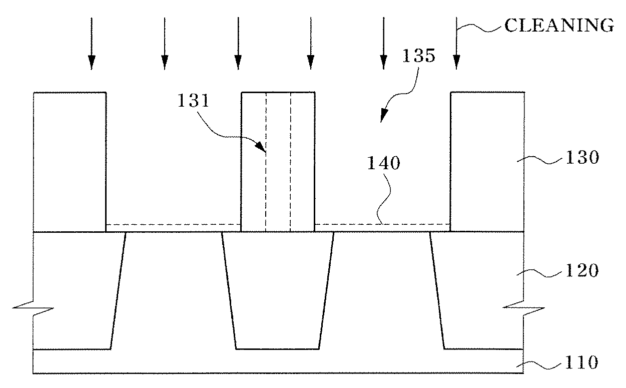
[0025]The invention is directed to a method for cleaning contaminants on the surface of cleaning target layers using an etchant including a fluorine (F)-containing species dispersed in an alcohol. The cleaning target layer may be a non-oxide layer, e.g., a mono crystalline silicon layer or a polycrystalline silicon layer such as a silicon substrate for example. The cleaning target may be native oxide created by spontaneous oxidation on the surface of the cleaning target layer. The cleaning target layer may be a silicon substrate, a polycrystalline silicon layer, an amorphous silicon layer, a tungsten (W) layer, a tungsten nitride (WN) layer, a tungsten silicide (WSix) layer, a titanium (Ti) layer, a titanium nitride (TiN) layer, a copper (Cu) layer, an aluminum (Al) layer, or a zinc (Zn) layer, for example.

[0026]Silicon oxide is an example of a native oxide. Native oxides have highly densified covalent bonds, when compared to silicon oxides formed by a deposition method such as chem...


PUM

PropertyMeasurementUnit
weightaaaaaaaaaa
conductiveaaaaaaaaaa
critical dimensionaaaaaaaaaa

Abstract

A method for fabricating a semiconductor device including surface cleaning includes forming a gate stack on a semiconductor substrate, cleaning contaminants present on the surface of the semiconductor substrate exposed through a contact hole using an etchant including a fluorine (F)-containing species dispersed in an alcohol, and filling a contact hole with a conductive layer to form a connection contact. The etchant preferably has a low selectivity of 1 or less.

Description

CROSS-REFERENCE TO RELATED APPLICATION[0001]The priority of Korean patent application number 10-2006-0078351, filed on Aug. 18, 2006, the disclosure of which is incorporated by reference in its entirety, is claimed.BACKGROUND[0002]The invention relates to a method for fabricating a semiconductor device. More specifically, the invention relates to a method for fabricating a semiconductor device including a surface cleaning step to remove contaminants (e.g., native oxides) from the surface of semiconductor device layers.[0003]With reductions in the design rule for semiconductor devices, supershort channel-type metal oxide semiconductor (MOS) transistors having a fine line critical dimension (CD) of 80 nm or less have been integrated on semiconductor substrates. In addition, the reduction in the design rule has introduced limitations in the process margin as well as restrictions on the removal of surface contaminants (e.g., native oxides) during the formation of connection wiring struc...

Claims


Application Information

Patent Timeline
Patent Type & Authority Applications(United States)
IPC IPC(8): H01L21/3205C23G1/02H01L21/4763
CPCC23G1/103H01L21/02063C23G1/125C23G1/106H01L21/302
Inventor LEE, SANG HO
Owner SK HYNIX INC
Why Eureka
Try Eureka