Junction formation on wafer substrates using group IV nanoparticles
A nanoparticle and wafer technology, applied in the field of nanoparticles, can solve the problems of limited manufacturing throughput, lack of simultaneous patterning, and constraints
- Summary
- Abstract
- Description
- Claims
- Application Information
AI Technical Summary
Problems solved by technology
Method used
Image

Examples
example 1
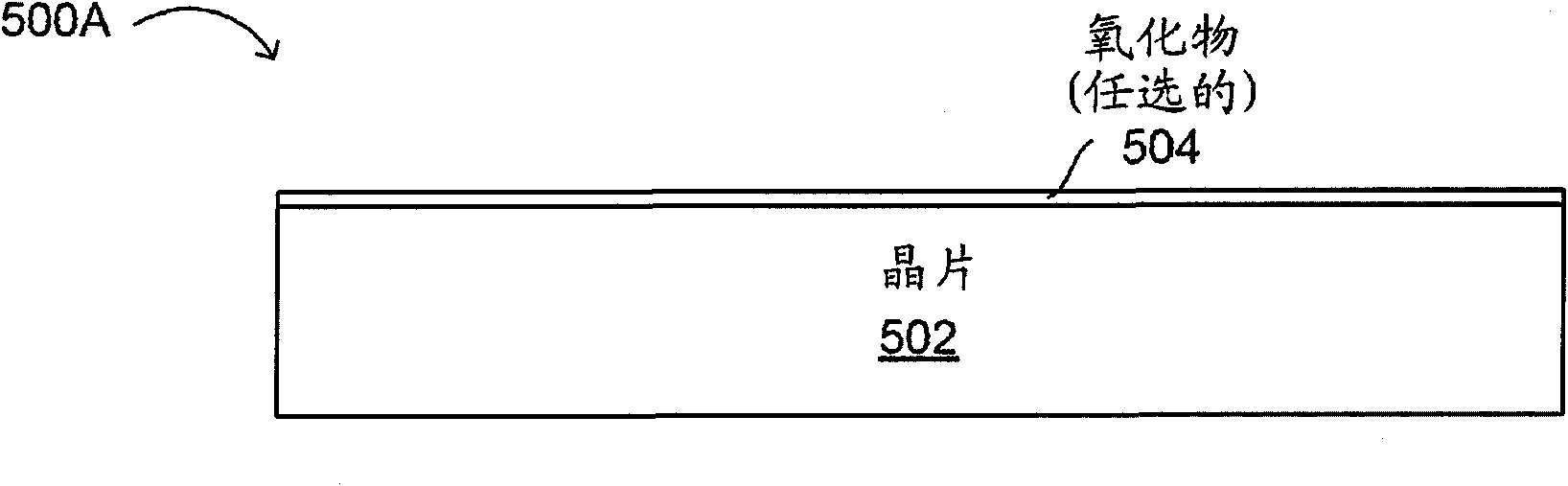
[0074]In this example, a 1 inch x 1 inch x 0.019 inch silicon wafer substrate doped with phosphorus to a resistivity of about 1 to 5 Ohmxcm was prepared by etching with NaOH, SC2, buffered oxide etch (BOE), and Piranha's Handle for cleaning.
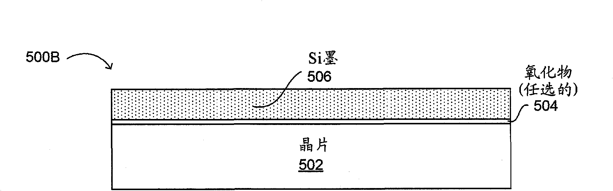
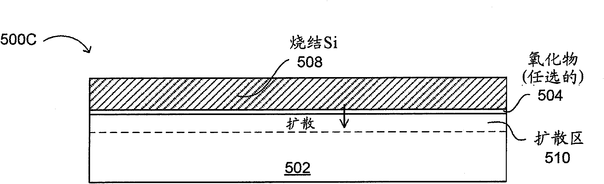
[0075] Additionally, a p-type silicon nanoparticle ink was prepared from approximately 10.0 nm + / - 0.5 nm silicon nanoparticles in an inert environment as a solution in pyridine at 5 mg / ml using a 15% power sonicated horn Sonicate it for 15 minutes. A sufficient amount of silicon nanoparticle ink was applied to substantially cover the wafer surface and spin-coated at 1000 rpm for 60 seconds to form a silicon nanoparticle porous dense body. After baking the layer on a hot plate at 100°C for 30 minutes in an inert environment, it was spin-coated at 1000 rpm for 60 seconds to form a second silicon nanoparticle porous dense body, and then in an inert environment on Bake at 100°C for 30 minutes on a hot plate. The thickness of the formed s...
PUM
| Property | Measurement | Unit |
|---|---|---|
| size | aaaaa | aaaaa |
| diameter | aaaaa | aaaaa |
| thickness | aaaaa | aaaaa |
Abstract
Description
Claims
Application Information
 - R&D Engineer
- R&D Manager
- IP Professional
- Industry Leading Data Capabilities
- Powerful AI technology
- Patent DNA Extraction
Browse by: Latest US Patents, China's latest patents, Technical Efficacy Thesaurus, Application Domain, Technology Topic.
© 2024 PatSnap. All rights reserved.Legal|Privacy policy|Modern Slavery Act Transparency Statement|Sitemap