Light-emitting device

A light-emitting device and electroluminescence technology, which are applied in the directions of instruments, electrical components, and electric solid-state devices, etc., can solve the problems of visual brightness differences and differences, and achieve the effect of suppressing brightness changes.

Inactive Publication Date: 2011-05-11
CANON KK
View PDF10 Cites 7 Cited by
  • Summary
  • Abstract
  • Description
  • Claims
  • Application Information

AI Technical Summary

Problems solved by technology

Luminance variation is a phenomenon in which luminance differs for the same input signal in an organic electroluminescent element, resulting in a difference in visual luminance

Method used


Image

  • Light-emitting device
  • Light-emitting device
  • Light-emitting device

Examples


no. 1 example

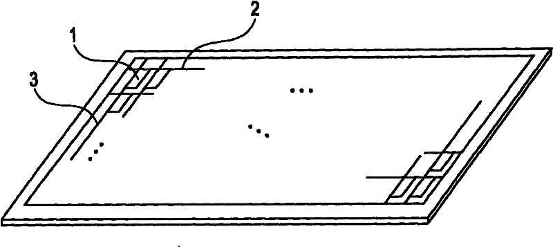
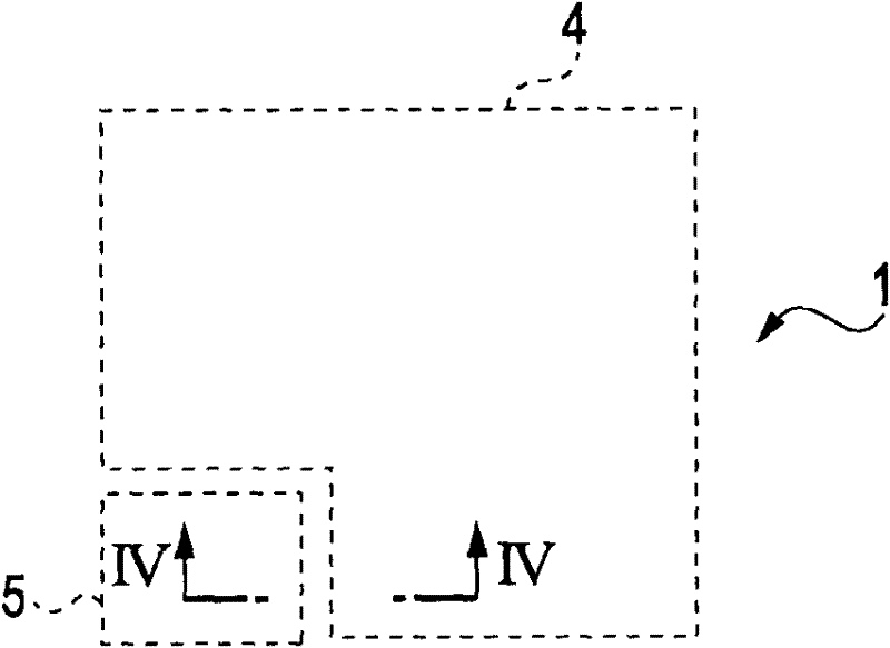
[0019] Embodiments of the present invention will be described with reference to the drawings. Figure 1A is a schematic perspective view of a light emitting device with multiple pixels. The pixel 1 is arranged near the intersection of a signal line 3 for sending a control signal to the pixel 1 and a selection line 2 for selecting the pixel 1 to which the control signal is sent. Figure 1B is a schematic plan view of the pixel 1 of the light emitting device according to this embodiment of the present invention. The pixel 1 is composed of a light-emitting region 4 in which an organic electroluminescence element is formed and a non-light-emitting region 5 in which a circuit for driving the organic electroluminescence element is formed. The light emitting area 4 of the pixel 1 includes an organic electroluminescent element and a holding capacitor for holding a control signal. The non-light-emitting area 5 of the pixel 1 includes a drive transistor for driving the organic electrol...

no. 2 example

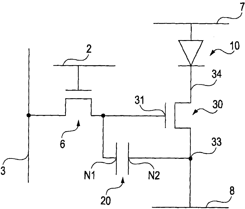
[0046] Figure 5A is a diagram of a circuit in a pixel of the second embodiment. The second embodiment differs from the first embodiment in that the terminal N2 of the holding capacitor 20 , which is different from the terminal N1 electrically connected to the gate electrode 31 of the driving transistor 30 , is connected to the potential line 9 which supplies a fixed potential. The terminal N2 of the holding capacitor 20 is regulated at a fixed potential via the potential line 9 .

[0047] electrically connected to the gate electrode 31 of the drive transistor 30 Figure 5A The terminal N1 of the holding capacitor 20 corresponds to the metal layer 21 , and the other terminal N2 of the holding capacitor 20 corresponds to the semiconductor layer 23 .

[0048] In the first embodiment, the signal voltage across the hold capacitor 20 is the voltage between the gate and source of the drive transistor 30 . Therefore, if the luminous intensity of the organic electroluminescent elem...


PUM


Abstract

A light-emitting device includes a plurality of pixels including an organic electroluminescent element, a drive transistor driving the organic electroluminescent element, and a hold capacitor holding a control signal for controlling the drive transistor, the organic electroluminescent element being electrically connected to one of a source electrode and a drain electrode of the drive transistor. The hold capacitor includes a metal layer, an insulating layer, and a semiconductor layer in this order. The semiconductor layer receives light emitted from the organic electroluminescent element. One of the metal layer and the semiconductor layer of the hold capacitor is electrically connected to a gate electrode of the drive transistor, and the other of the metal layer and the semiconductor layer of the hold capacitor is specified at a fixed potential.

Description

technical field [0001] The present invention relates to a light-emitting device having a plurality of organic electroluminescence elements, and particularly to a light-emitting device in which variations in luminance are suppressed. Background technique [0002] A light-emitting device having a plurality of organic electroluminescent elements has attracted great attention as a self-luminous device that is expected to be thinner and consume less power. The organic electroluminescent element has an organic compound layer between an anode and a cathode, and emits light using energy generated when electrons and holes respectively injected into the organic compound layer from the cathode and anode are recombined. [0003] It is known that an organic electroluminescence element exhibits deterioration such as a reduction in luminance as driving time elapses so that the driving voltage is increased. Since this degradation differs from organic electroluminescent element to organic e...

Claims


Application Information

Patent Timeline
Patent Type & Authority Applications(China)
IPC IPC(8): G09G3/32H01L27/32
CPCG09G3/3233G09G2300/0842G09G2320/0233G09G2320/0295G09G2360/141G09G2360/142H10K59/1216H10K59/13
Inventor 田村正浩高林明治池田宏治
Owner CANON KK
Why Eureka
Try Eureka