Pixel structure

A pixel structure and pixel electrode technology, applied in optics, instruments, electrical components, etc., can solve the problems of reduced aperture ratio and reduced display quality of liquid crystal display devices, so that the aperture ratio will not be reduced, and the uneven brightness of the picture can be improved. Effects of Different Pixel Gate-Drain Parasitic Capacitance Cgd Different Problems

Active Publication Date: 2011-05-18
CENTURY DISPLAY (SHENZHEN) CO LTD
View PDF3 Cites 9 Cited by
  • Summary
  • Abstract
  • Description
  • Claims
  • Application Information

AI Technical Summary

Problems solved by technology

Since the gate 130 and the area between the gate 130 and the data line 120 are generally opaque, and the area between the gate 140 and the data line 120 in the pixel structure 100 is enlarged, therefore, the present application Compared with the general pixel structure, the aperture ratio of the pixel structure 100 is reduced, thus, the display quality of the liquid crystal display device is reduced.

Method used


Image

  • Pixel structure
  • Pixel structure
  • Pixel structure

Examples


no. 1 example

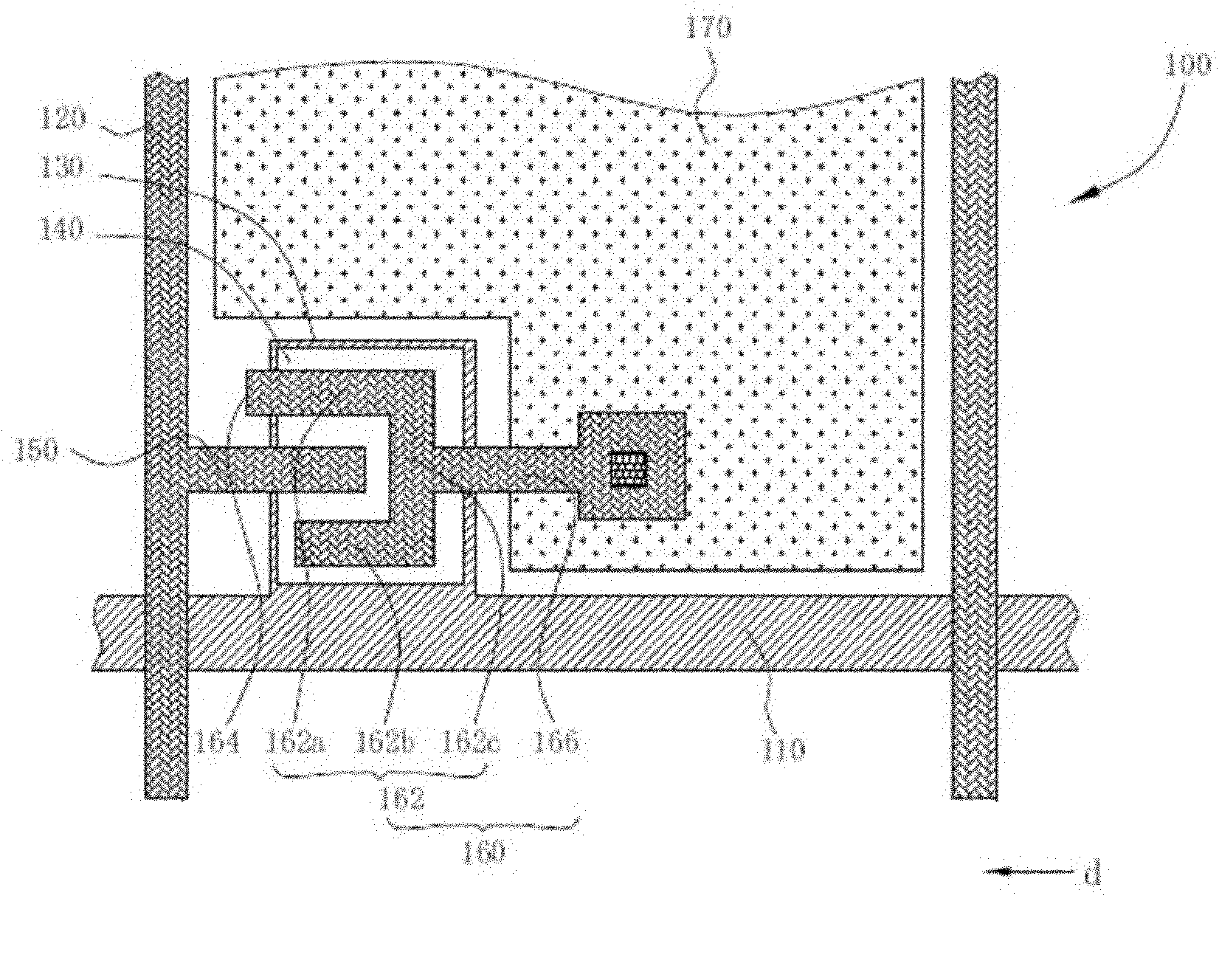
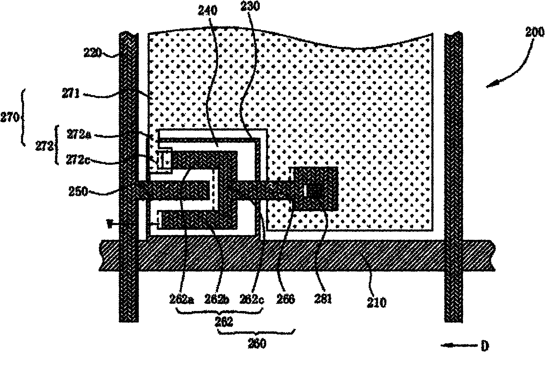
[0036] figure 2 is a partial top view schematic diagram of the pixel structure of the first embodiment of the present invention, please refer to figure 2 The pixel structure 200 includes a scan line 210 , a data line 220 , a gate 230 , a semiconductor layer 240 , a source 250 , a drain 260 and a pixel electrode 270 . The scan lines 210 and the data lines 220 intersect each other and are electrically insulated. The gate 230 and the scan line 210 are the first metal layer, and the gate 230 is electrically connected to the scan line 210 . The semiconductor layer 240 is located above the gate 230 . The data line 220 , the source 250 and the drain 260 are the second metal layer, and the source 250 is electrically connected to the data line 220 , and both the source 250 and the drain 260 are at least partially located on the gate 230 . In this embodiment, the gate 230 , the semiconductor layer 240 , the source 250 and the drain 260 can form a thin film transistor (not shown). ...

no. 2 example

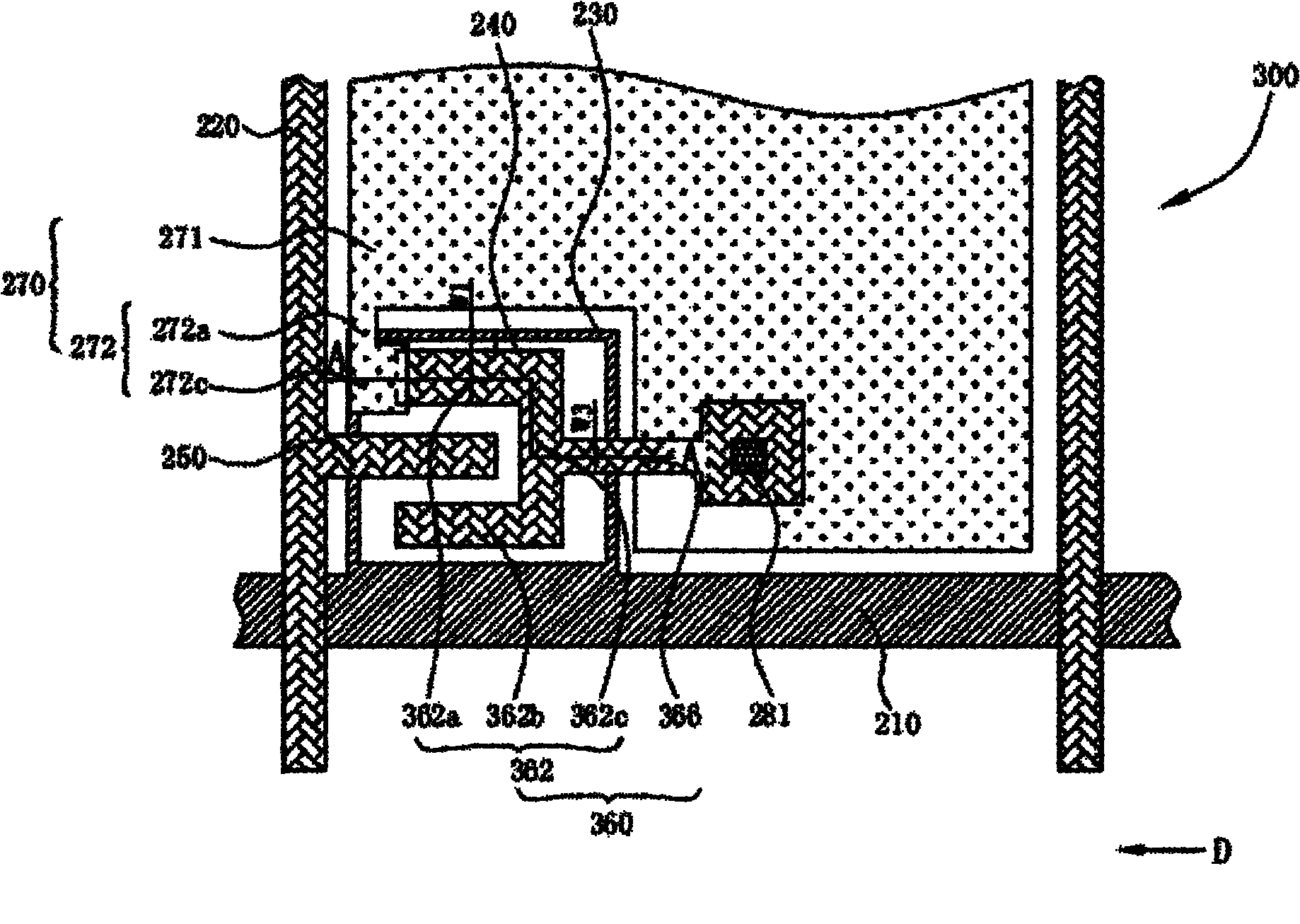
[0046] image 3 is a partial top view diagram of the pixel structure of the second embodiment of the present invention, image 3 The pixel structure and figure 2 The pixel structure is similar, so the same reference numerals represent the same components. The difference between this embodiment and the first embodiment is the design of the drain 360 of the pixel structure 300 .

[0047] Specifically, the difference between the drain 360 of this embodiment and the drain 260 of the first embodiment is that the width W1 of the first branch 362a of the comb-shaped portion 362 is not equal to the width W3 of the connecting portion, and the relationship is satisfied: W1 is substantially 1.4 times of W3. When the width W1 of the first branch 362a and the width W3 of the connecting portion satisfy this relationship, it can be obtained that the variation of the parasitic capacitance between the gate 230 and the extension branch 272c is equal to the variation of the parasitic capacit...

no. 3 example

[0056] Figure 5 is a schematic partial top view of the pixel structure of the third embodiment of the present invention, Figure 5 The pixel structure and figure 2 The pixel structure is similar, so the same reference numerals represent the same components. The difference between this embodiment and the first embodiment is the design of the pixel electrode 470 of the pixel structure 400 .

[0057] Specifically, the difference between the pixel electrode 470 of this embodiment and the pixel electrode 270 of the second embodiment is that the width W4 of the extension branch 472c of the pixel electrode 470 is smaller than the width W1 of the first branch 262a, and the overlapping portion of the extension branch 472c is completely placed Inside the first branch 262a, that is, the first branch 262a completely covers the extension branch 472c in the region of the overlapping portion. Likewise, the design of this embodiment can improve the difference in gate-drain parasitic capa...


PUM


Abstract

The invention provides a pixel structure comprising a scanning line, a data line, a grid electrode, a source electrode, a drain electrode and a pixel electrode, wherein the scanning wire and the data line are staggered with each other and electrically insulated; the grid electrode is electrically connected with the scanning line; at least part of the source electrode is positioned on the grid electrode and connected to the data line; the drain electrode is at least partially positioned on the grid electrode and opposite to the source electrode; and the pixel electrode comprises a main body part and an extended part, the main body part is electrically connected with the drain electrode, the extended part is electrically connected with the main body part, and the extended part is partially overlapped with the grid electrode and the drain electrode.

Description

【Technical field】 [0001] The invention relates to a pixel structure of a liquid crystal display device, and in particular to a pixel structure capable of compensating parasitic capacitance without reducing the aperture ratio. 【Background technique】 [0002] A general thin film transistor liquid crystal display is mainly composed of a thin film transistor array substrate, a counter substrate and a liquid crystal layer sandwiched between the two substrates. The thin film transistor array substrate mainly includes a plurality of scanning lines, a plurality of data lines, thin film transistors arranged between the scanning lines and the data lines, and a pixel electrode (Pixel Electrode) corresponding to each thin film transistor. The above-mentioned thin film transistor includes a gate, a semiconductor layer, a source and a drain, which are used as switching elements of the liquid crystal display unit. [0003] The manufacturing process of the thin film transistor array substr...

Claims


Application Information

Patent Timeline
Patent Type & Authority Applications(China)
IPC IPC(8): G02F1/1362G02F1/1343H01L27/02
Inventor 柳智忠曹岩
Owner CENTURY DISPLAY (SHENZHEN) CO LTD
Why Eureka
Try Eureka