Optical analyzer and wavelength stabilized laser device for analyzer
A laser device and optical analysis technology, which is applied in the direction of material analysis, lasers, and analytical materials through optical means, can solve the problems of narrow laser wavelength band, reduced analysis accuracy, and weakened light intensity, so as to achieve consistent absorption wavelength and flexibility Improve and improve the effect of vulnerability
- Summary
- Abstract
- Description
- Claims
- Application Information
AI Technical Summary
Problems solved by technology
Method used
Image

Examples
no. 1 example
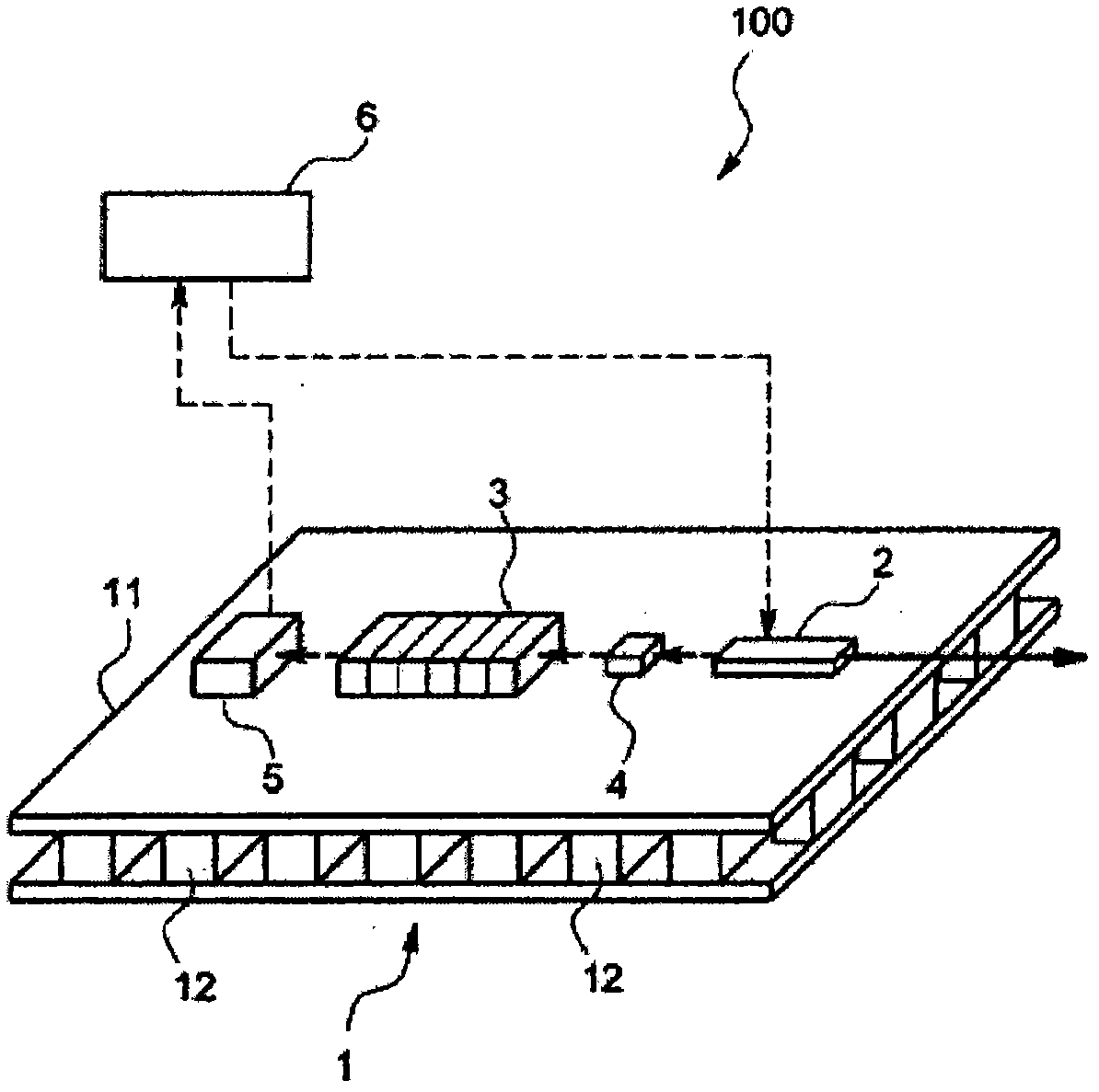
[0082] The analyzer laser device 100 according to the first embodiment is used, for example, in an infrared gas analyzer for measuring the component concentration of an analyte in a sample gas, and has such figure 1 structure shown.
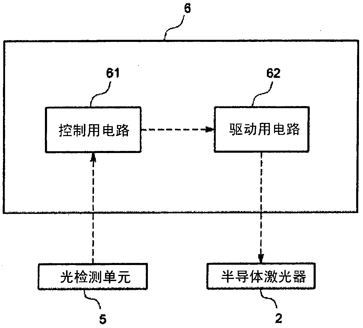
[0083] exist figure 1 In , the symbol 1 represents the Peltier module. This Peltier module 1 has a flat single substrate 11 and a Peltier element 12 mounted on the back surface of the substrate 11 . Here, a sensor and control circuit (not shown) such as a thermostat for operating the Peltier element 12 to keep the surface temperature of the substrate 11 constant is attached.
[0084] Reference numeral 2 denotes a semiconductor laser that outputs infrared laser light for gas analysis. The semiconductor laser 2 outputs analytical laser light in the mid-infrared region (approximately 2.5 μm to 20 μm) from the main injection port, and emits leaked light having the same wavelength as the analytical laser light and having a certain proportional inte...
no. 2 example
[0110] Next, a second embodiment will be described. Also, the symbols added in the second embodiment and the symbols added in the first embodiment are independent of each other and have no correlation.
[0111] The optical analysis device X100 designed in this second embodiment, for example, is used to detect the water vapor (H 2 O) the infrared gas analysis device of concentration, it has such as Figure 7 structure shown.
[0112] in the Figure 7 In , symbol X1 denotes a semiconductor laser that emits infrared rays as measurement light for gas analysis. Here, the emission near-infrared region (about 0.8 μm to about 2.5 μm, due to the determination of H in this embodiment 2 O concentration, eg, 1390nm) coherent light (hereinafter also referred to as laser) laser.
[0113] Symbol X2 denotes a fiber type analysis section exposed to sample gas. The fiber type analysis section X2, such as Figure 8 , Figure 9 As shown, it is composed of a core X2a and a cladding X2b. At...
PUM
 Abstract
Description
Claims
Application Information
 - R&D Engineer
- R&D Manager
- IP Professional
- Industry Leading Data Capabilities
- Powerful AI technology
- Patent DNA Extraction
Browse by: Latest US Patents, China's latest patents, Technical Efficacy Thesaurus, Application Domain, Technology Topic.
© 2024 PatSnap. All rights reserved.Legal|Privacy policy|Modern Slavery Act Transparency Statement|Sitemap