Memory module and auxiliary module for memory
A technology of memory modules and auxiliary modules, applied in the fields of instrumentation, memory address/allocation/relocation, electrical digital data processing, etc.
- Summary
- Abstract
- Description
- Claims
- Application Information
AI Technical Summary
Problems solved by technology
Method used
Image

Examples
no. 1 example
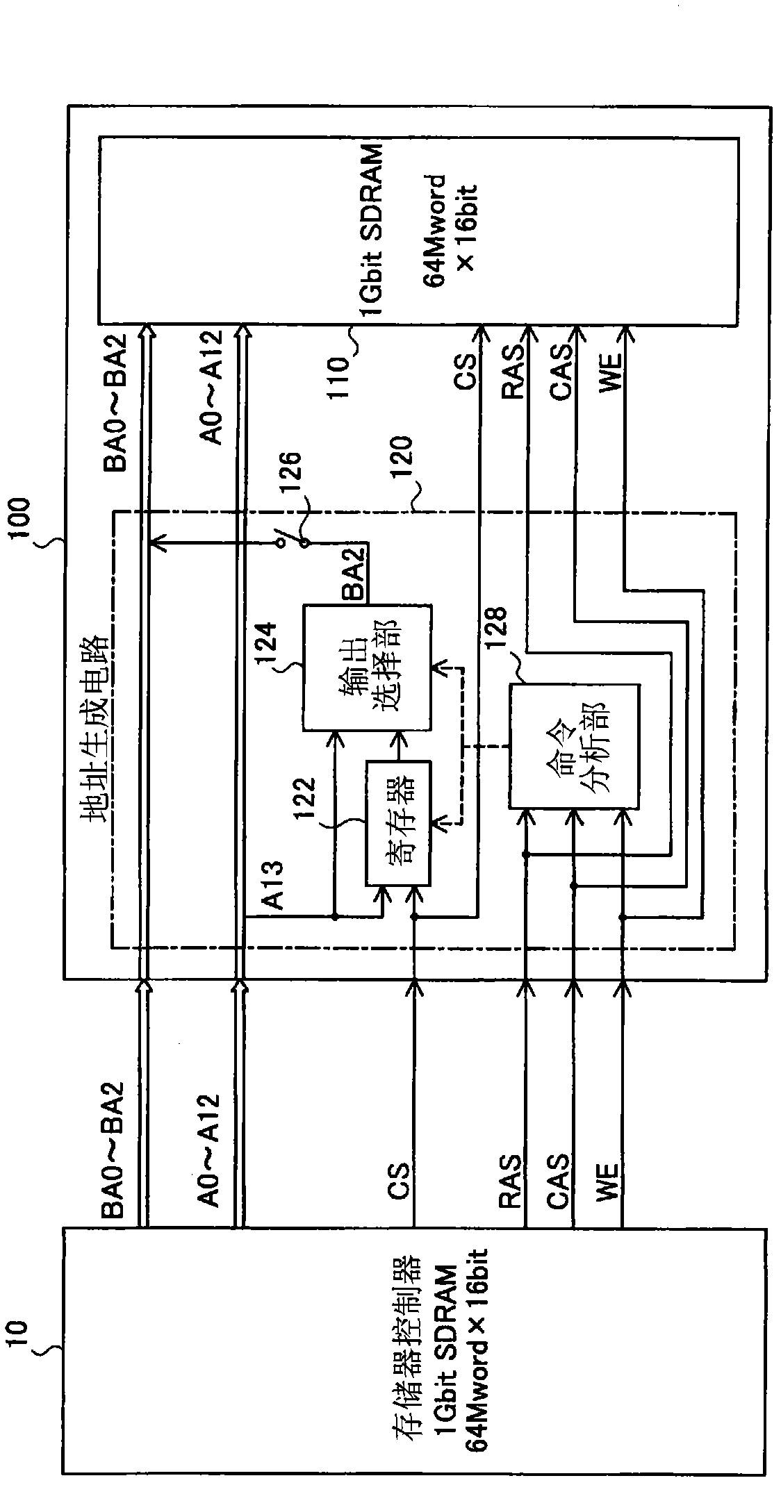
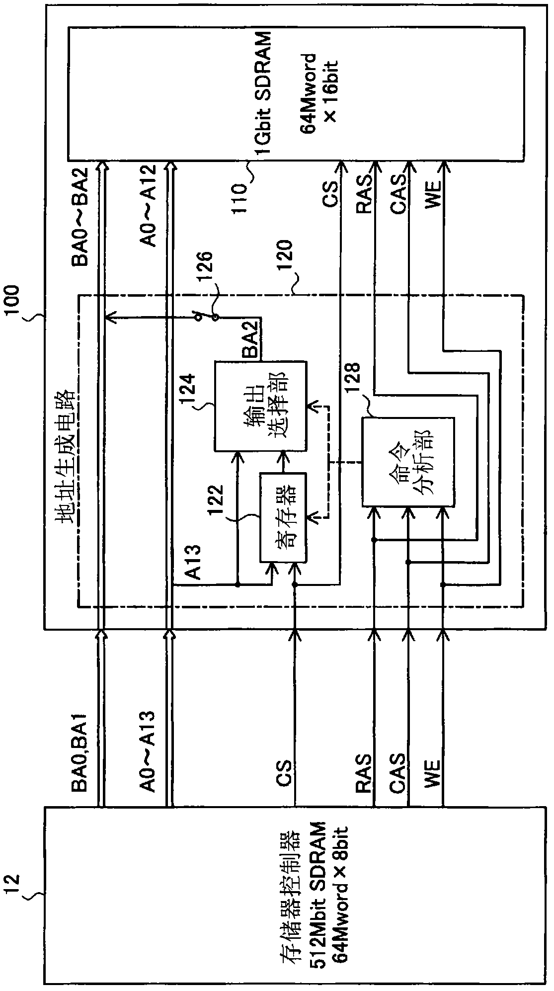
[0066] figure 1 and figure 2 It is an explanatory diagram showing a schematic configuration of the memory module 100 as the first embodiment of the present invention. figure 1 A state when the memory module 100 is connected to the memory controller 10 is shown in . In addition, in figure 2 The state when the memory module 100 is connected to the memory controller 12 is shown in . Their differences are explained later.
[0067] As shown in the figure, this memory module 100 includes an SDRAM 110 and an address generation circuit 120 . In this embodiment, a 1 Gbit (64 Mword×16 bit) DDR2 (Double Data Rate 2: Double Data Rate 2) SDRAM is used as the SDRAM 110 . As will be described later, the inside of the SDRAM 110 is divided into eight banks, and each bank can operate independently. In addition, a 3-bit bank address (BA0 to BA2), a 13-bit row address (A0 to A12), and a 10-bit column address (A0 to A9) are input into the SDRAM 110, and an access target is specified based ...
no. 2 example
[0093] Figure 7 It is an explanatory diagram showing a schematic configuration of a memory auxiliary module 200 as a second embodiment of the present invention.
[0094] This memory auxiliary module 200 is used when the user wants to operate the SDRAM 110 included in the memory module 100A by using the memory controller 12 that does not support the SDRAM 110 . Such as Figure 7 As shown, the auxiliary module 200 for memory is connected to the memory controller 12 and the memory module 100A, and relays the exchange of signals and data between the memory controller 12 and the memory module 100A. Also, the memory module 100A is derived from the memory module 100 of the first embodiment (refer to figure 1 , figure 2 ) is a memory module obtained by removing the address generating circuit 120. Other parts of the memory module 100A are the same as the memory module 100 of the first embodiment.
[0095] The memory auxiliary module 200 is an adapter including the address gener...
Deformed example 1
[0102] Figure 8 It is an explanatory diagram showing a schematic configuration of a memory module 100B as a first modified example. The memory module 100 of the first embodiment described before (refer to figure 1 , figure 2 ), the chip select signal (CS) is input to the register 122 included in the address generation circuit 120, and the register 122 determines the command input from the command analysis unit 128 at the falling edge of the input chip select signal (CS). In contrast, in the memory module 100B of this embodiment, a chip select signal (CS) is input to the command analysis unit 128B included in the address generation circuit 120B. The command analysis unit 128B analyzes the command at the falling edge of the input chip select signal (CS), determines the command, and outputs the determined command to the register 122B and the output selection unit 124 .
[0103] Other parts of the memory module 100B of Modification 1 are the same as those of the memory modul...
PUM
 Abstract
Description
Claims
Application Information
 - R&D Engineer
- R&D Manager
- IP Professional
- Industry Leading Data Capabilities
- Powerful AI technology
- Patent DNA Extraction
Browse by: Latest US Patents, China's latest patents, Technical Efficacy Thesaurus, Application Domain, Technology Topic.
© 2024 PatSnap. All rights reserved.Legal|Privacy policy|Modern Slavery Act Transparency Statement|Sitemap