Metadata rebuild in a flash memory controller following a loss of power

a flash memory controller and power loss technology, applied in the field of data storage, can solve the problems of reducing the effective and usable capacity of each drive to as low as 12 gb per drive, affecting the performance of the flash memory controller, so as to achieve the effect of maximizing the use of the host, reducing the cost of operation, and effectively masking the write latencies inherent in the hardwar

Active Publication Date: 2009-07-02
SANDISK TECH LLC
View PDF75 Cites 198 Cited by
  • Summary
  • Abstract
  • Description
  • Claims
  • Application Information

AI Technical Summary

Benefits of technology

[0012]In one embodiment, the described solution to the performance limitations of flash memory involves the use of multiple microprocessors in the controller design, thereby creating multiple parallel independent pipelines, each of which is capable of handling a portion of a single transaction. This design maximizes use of the host and flash interfaces, and allows individual transactions to be broken up into many small portions, which can be reordered and handled in parallel to increase performance. The architecture is designed to allow multiple processors to perform their functions without the use of costly and inefficient interrupts.
[0013]The use of parallel pipelines allows the controller to effectively mask the write latencies inherent in the use of flash memory. In addition, the use of multiple independent processors provides sufficient processing power to handle overhead imposed by solutions to the endurance and error problems described above. By breaking host-initiated transactions into a large number of independent flash reads and writes, the controller architecture described herein allows for a high level of performance that is impossible using conventional controller designs.

Problems solved by technology

The constraints of the head / media technology limit the read / write capabilities to only one active head at a time.
This has had the effect of reducing the effective and usable capacity of each drive to as low as 12 GB per drive, even though these devices are available at up to 450 GB capacities.
The lower capacity, in turn, has exacerbated floor space, cooling and power issues, all of which have become extremely problematic for enterprise-level mass storage systems.
However, although the smaller form factor allows for a larger number of drives in the same space, the serial nature of hard drive operations means that even smaller form factor drives present serious space, cooling and power problems.
Nevertheless, flash memory has not traditionally been used in such environments due to certain technical constraints.
The first technical problem is write speed, which may be as slow as one-tenth that of a mechanical hard drive.
This results from the fact that data cannot be overwritten on a NAND flash device without a long erase cycle prior to the write.
Because the erase cycle directly affects the write performance, most flash designs move the write data to a new location and delay the erase until later.
In a busy system, delayed erase cycles may build up until the processor runs out of free flash pages and has to stop to create new ones, thereby significantly affecting system performance.
The second technical problem is the specified limit for each flash memory page of 100,000 erase cycles for Single Level Cell (“SLC”) devices and 10,000 cycles for Multi-Level Cell (“MLC”) devices.
These pose particular problems for datacenters that operate with unpredictable data streams that may cause “hot spots,” resulting in certain highly-used areas of memory being subject to a large number of erases.
The third issue is data loss, which can occur as the result of various factors affecting flash memory, including read disturbs or program disturbs, which lead to the loss of data bits caused by the reading or writing of memory cells adjacent to the disturbed cell.
The state of a flash memory cell may also change in an unpredictable manner as the result of the passage of time.
These technical problems create serious issues for the use of flash memory in high-capacity, high-performance storage applications.
In each case, technical solutions exist, but the solutions place significant strain on the processing power available in standard flash memory controllers, which generally include a single processor.
That strain makes it difficult to overcome these technical problems in these environments.

Method used


Image

  • Metadata rebuild in a flash memory controller following a loss of power
  • Metadata rebuild in a flash memory controller following a loss of power
  • Metadata rebuild in a flash memory controller following a loss of power

Examples


Embodiment Construction

I. Overview.

[0072]A. System Overview.

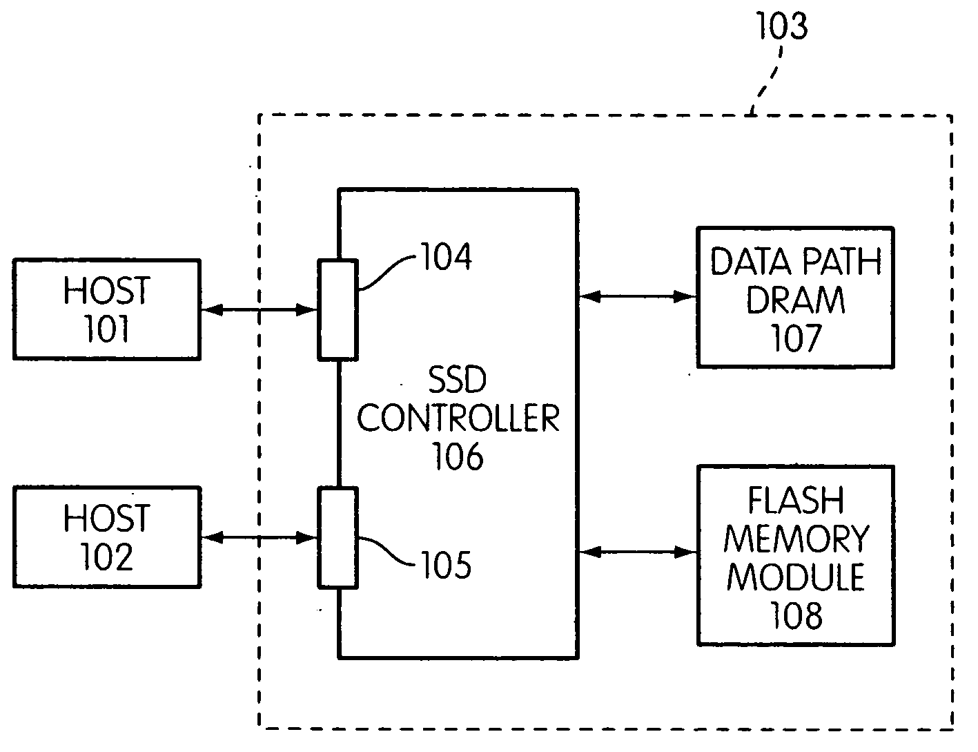
[0073]In the currently preferred embodiment, the system described herein is designed to operate with various enterprise-level mass storage protocols, including SAS (“Serial Attached SCSI”), FC (“Fibre Channel”) and FC-AL (“Fibre Channel Arbitrated Loop), all of which are based on the Small Computer Systems Interface (“SCSI”), and Serial ATA (“SATA”) protocols. These protocols are highly familiar to those of ordinary skill in the art, and will not be further described herein. Except where particular protocols are called out, the systems and methods disclosed herein do not depend on the particular protocol being used and are designed to operate correctly with all of them. Moreover, these systems and methods may be adapted for use with other similar protocols, either currently in use or not yet developed, including protocols designed for enterprise-level applications as well as protocols designed for other applications, such as end-user.

[0074]As a m...


PUM


Abstract

A method of rebuilding metadata in a flash memory controller following a loss of power. The method includes reading logical address information associated with an area of flash memory, and using time stamp information to determine if data stored in the flash memory area is valid.

Description

CROSS-REFERENCE TO RELATED APPLICATIONS[0001]This application claims priority to U.S. Provisional Patent Application No. 61 / 017,123 filed Dec. 27, 2007, the disclosure of which is incorporated herein by reference, as if fully stated here, for all purposes.[0002]The present application contains subject matter related to the subject matter in the following copending patent applications: U.S. patent application Ser. No. M-17228-01 US, filed on even date herewith and entitled “System and Method for Performing Host Initiated Mass Storage Commands Using a Hierarchy of Data Structures;” U.S. patent application Ser. No. M-17228-02 US, filed on even date herewith and entitled “Flash Memory Controller Having Reduced Pinout;” U.S. patent application Ser. No. M-17228-03 US, filed on even date herewith and entitled “Multiprocessor Storage Controller;” U.S. patent application Ser. No. M-17228-04 US, filed on even date herewith and entitled “Storage Controller for Flash Memory Including a Crossbar...

Claims


Application Information

Patent Timeline
Patent Type & Authority Applications(United States)
IPC IPC(8): G06F12/00
CPCG06F13/1657G11C7/1051G06F2212/7201G11C16/10G06F12/0246G11C7/1063G06F3/0604G06F3/0659G06F3/0679G06F13/28G06F2212/7203G06F2212/7205
Inventor OLBRICH, AARON K.PRINS, DOUGLAS A.
Owner SANDISK TECH LLC
Why Eureka
Try Eureka