Memory system and memory card

a memory system and memory card technology, applied in the field of memory system and memory card, can solve the problems of increasing the size and the relative long processing time required, etc., and achieve the reduction of the number of nonvolatile memory chips required to construct the memory card, the reduction of the effect of reducing the cost of the memory card

Inactive Publication Date: 2005-01-20
RENESAS ELECTRONICS CORP
View PDF8 Cites 194 Cited by
  • Summary
  • Abstract
  • Description
  • Claims
  • Application Information

AI Technical Summary

Benefits of technology

[0024] Also in the memory card, in a manner similar to the above, in the simultaneous writing operation, the writing operation much longer than the write setup time can be performed perfectly in parallel. In the interleave writing operation, the writing operation following the write setup of one memory bank can be performed sequentially so as to partially

Problems solved by technology

To obtain a desired threshold voltage in the memory cell transistor, relatively long processing time is required.
However, in the conventional method of performing interleave writing

Method used


Image

  • Memory system and memory card
  • Memory system and memory card
  • Memory system and memory card

Examples


Embodiment Construction

[0061] Memory System

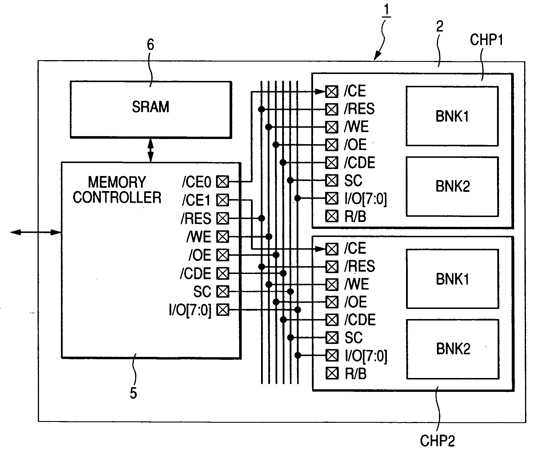
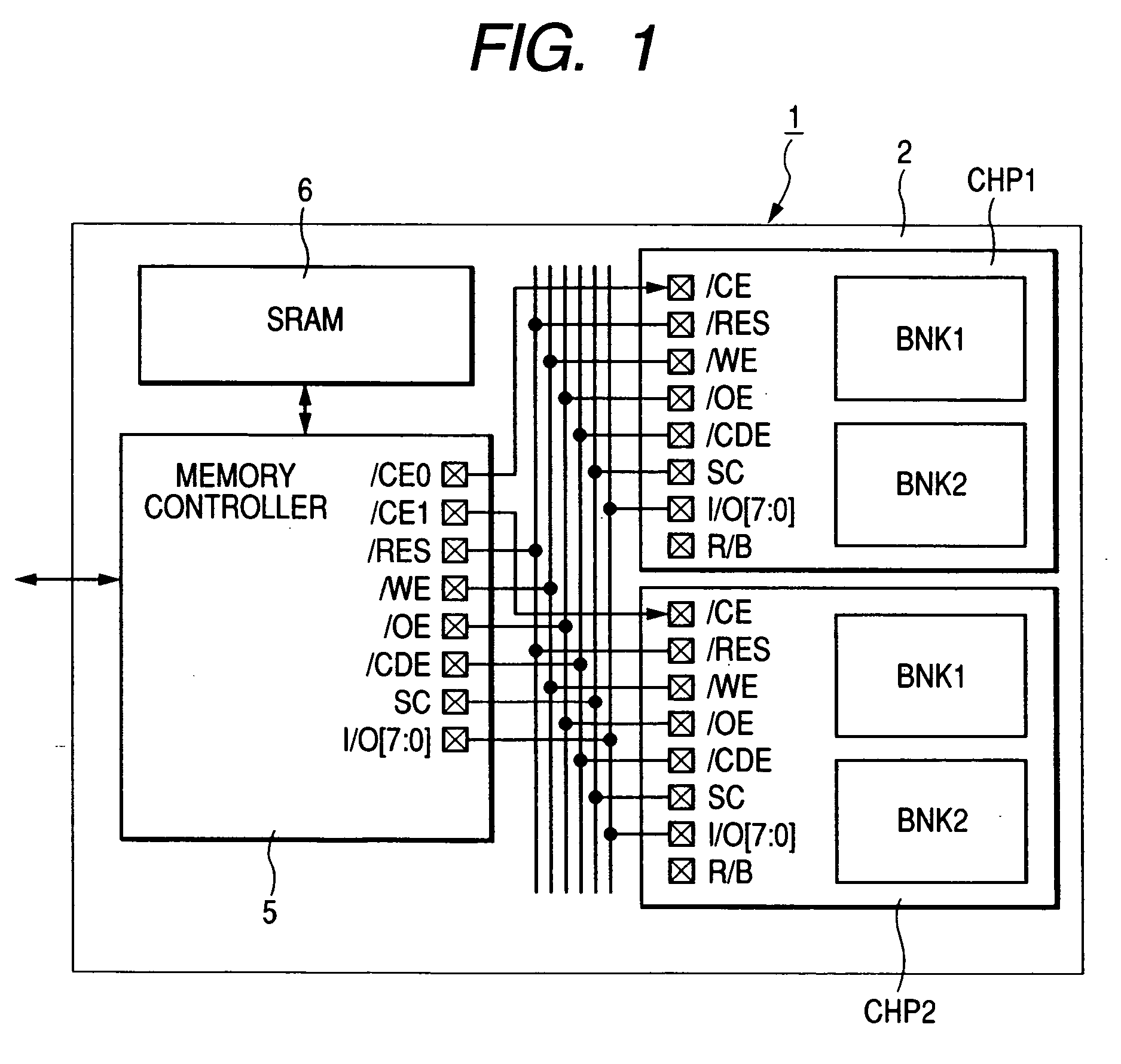
[0062]FIG. 1 shows a memory card as an example of a memory system according to the invention. A memory card 1 shown in the diagram has, on a card board 2, plural nonvolatile memory chips, for example, two flash memory chips CHP1 and CHP2 each having plural, for example, two memory banks BNK1 and BNK2 which can operate independently of each other, a memory controller 5 which can control an access to each of the flash memory chips CHP1 and CHP2, and an SRAM 6 connected to the memory controller 5. The SRAM 6 can be used as a data buffer for temporarily storing write data onto the flash memory chips CHP1 and CHP2. The memory controller 5 can selectively instruct the simultaneous writing operation or interleave writing operation on the memory banks BNK1 and BNK2 of the flash memory chips CHP1 and CHP2.

[0063] The details of the flash memory chips CHP1 and CHP2 will be described later. The functions for responding to the instruction of the simultaneous writing operati...


PUM


Abstract

A memory system includes a plurality of nonvolatile memory chips (CHP1 and CHP2) each having a plurality of memory banks (BNK1 and BNK2) which can perform a memory operation independent of each other and a memory controller (5) which can control to access each of said nonvolatile memory chips. The memory controller can selectively instruct either a simultaneous writing operation or an interleave writing operation on a plurality of memory banks of the nonvolatile memory chips. Therefore, in the simultaneous writing operation, the writing operation which is much longer than the write setup time can be performed perfectly in parallel. In the interleave writing operation, the writing operation following the write setup can be performed so as to partially overlap the writing operation on another memory bank. As a result, the number of nonvolatile memory chips constructing the memory system of the high-speed writing operation can be made relatively small.

Description

TECHNICAL FIELD [0001] The present invention relates to a memory system and a memory card each using a plurality of chips of nonvolatile memories such as flash memories having multiple banks and relates to a technique effective when applied to a memory card such as a multimedia card. BACKGROUND ART [0002] A flash memory can store information in accordance with a threshold voltage changed by injecting or discharging electrons to / from a floating gate or the like of a memory cell transistor. In the specification, a state where the threshold voltage of the memory cell transistor is low will be called an erase state, and a state where the threshold voltage is high will be called a write state. In the case of storing information in accordance with write data, a high voltage is applied to a memory cell transistor in the erase state in accordance with a logic value of the write data. To obtain a desired threshold voltage in the memory cell transistor, relatively long processing time is requ...

Claims


Application Information

Patent Timeline
IPC IPC(8): G06F12/00G06F12/06G06F13/16G11C7/10G11C16/02G11C16/10
CPCG06F13/1647G11C7/1042G11C2216/14G11C16/10G11C16/32G11C7/1045
Inventor HORII, TAKASHIYOSHIDA, KEIICHINOZOE, ATSUSHI
Owner RENESAS ELECTRONICS CORP
Why Eureka
Try Eureka