Apparatus including an overlay mark and method of producing semiconductor assembly

A technology for alignment marks and semiconductors, applied in semiconductor devices, semiconductor/solid-state device manufacturing, electric solid-state devices, etc., can solve problems such as small geometric size, chip failure, and inability to measure the alignment amount, so as to achieve precise and accurate alignment , The effect of chip yield improvement

Active Publication Date: 2013-05-08
TAIWAN SEMICON MFG CO LTD
View PDF5 Cites 0 Cited by
  • Summary
  • Abstract
  • Description
  • Claims
  • Application Information

AI Technical Summary

Problems solved by technology

However, as geometries become smaller, existing alignment marks may not measure actual alignment between layers
As a result, alignment error measurements may be inaccurate, resulting in more die failures
[0004] In light of this, while existing alignment marks are generally adequate for their intended purpose, they are not entirely satisfactory in every respect

Method used


Image

  • Apparatus including an overlay mark and method of producing semiconductor assembly
  • Apparatus including an overlay mark and method of producing semiconductor assembly
  • Apparatus including an overlay mark and method of producing semiconductor assembly

Examples


Embodiment Construction

[0128] It should be understood that the present disclosure provides many different embodiments, or examples, by which various features of the invention can be implemented. Specific examples of components and arrangements are disclosed below to simplify the description of the present invention. Of course, these are just examples and are not intended to limit the present invention. In addition, forming the first feature on or over the second feature of the present invention may include various embodiments where the first and second features are formed in direct contact, and may include intercalating formation of the first and second features. Multiple embodiments of additional features between such that the first and second features are not in direct contact. Various features may be arbitrarily drawn in different scales for simplicity and clarity.

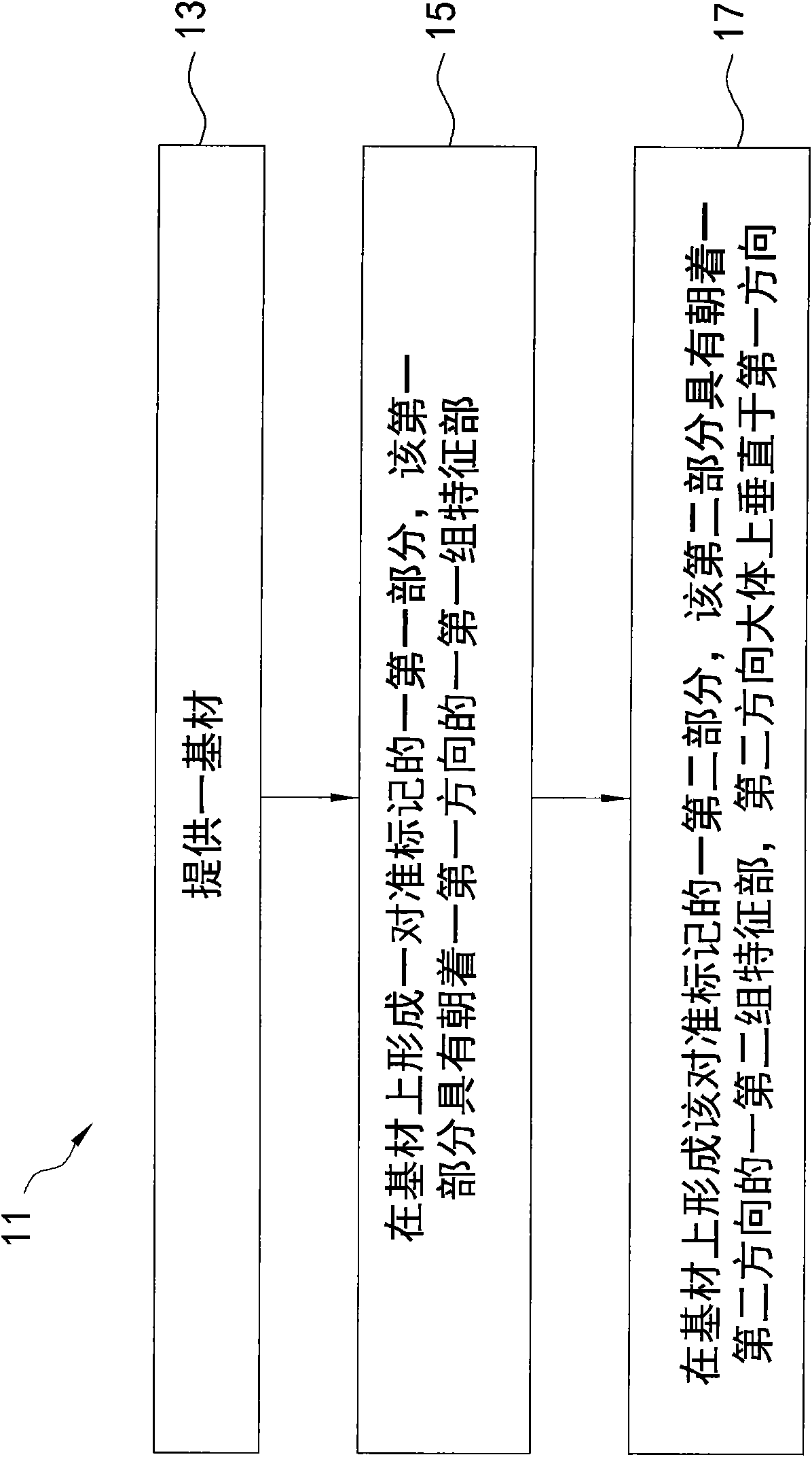
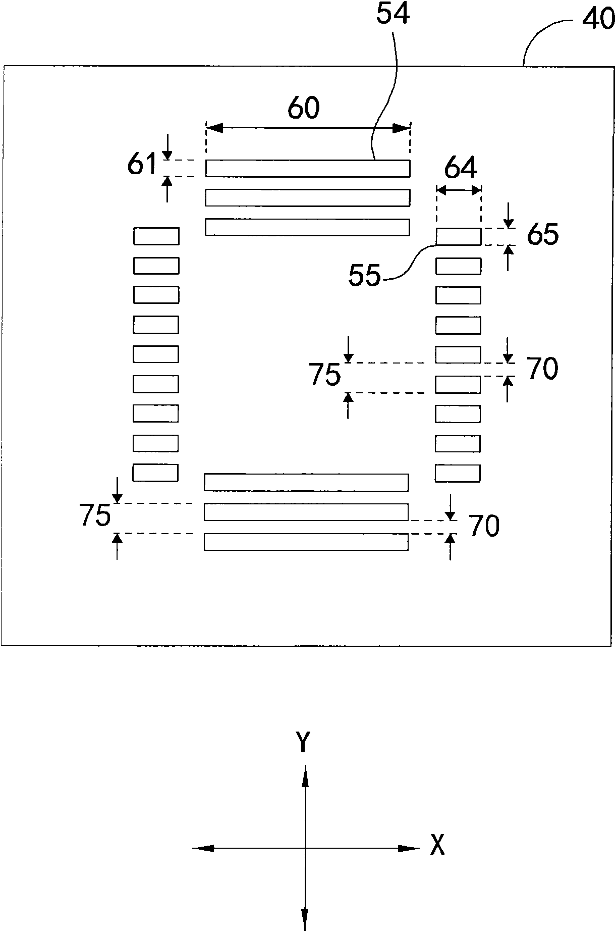
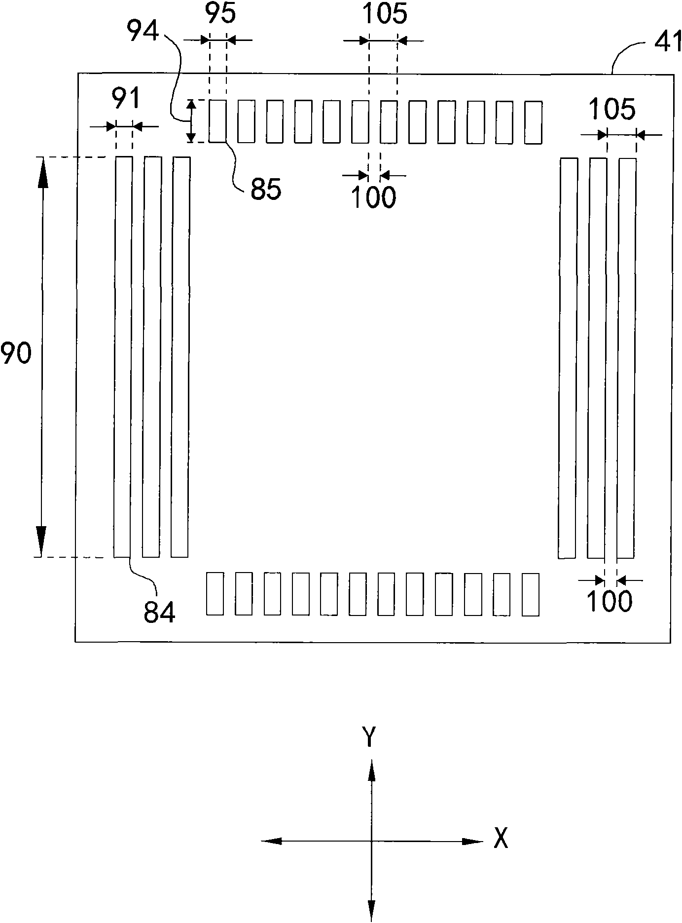
[0129] figure 1 Shown is a flowchart of a method for manufacturing alignment marks according to various aspects disclosed in the...


PUM


Abstract

Provided is an apparatus that includes an overlay mark. The overlay mark includes a first portion that includes a plurality of first features. Each of the first features have a first dimension measured in a first direction and a second dimension measured in a second direction that is approximately perpendicular to the first direction. The second dimension is greater than the first dimension. The overlay mark also includes a second portion that includes a plurality of second features. Each of the second features have a third dimension measured in the first direction and a fourth dimension measured in the second direction. The fourth dimension is less than the third dimension. At least one of the second features is partially surrounded by the plurality of first features in both the first and second directions.

Description

technical field [0001] The invention relates to a semiconductor component, in particular to an alignment mark used in a photoetching process. Background technique [0002] The semiconductor integrated circuit (IC) industry has experienced rapid growth. Technological improvements in IC materials and design have spawned many generations of ICs, each with smaller and more complex circuits than the previous generation. However, these improvements also increase the complexity of the process and the complexity of manufacturing the IC, and similar developments in IC process and manufacturing are necessary for these improvements to be realized. During the evolution of integrated circuits, functional density (ie, the number of interconnected components per chip area) generally increases while geometry size (ie, the smallest component (or line) created using a fabrication process) decreases. [0003] Small geometries set stricter requirements in the photolithographic etch process. ...

Claims


Application Information

Patent Timeline
Patent Type & Authority Patents(China)
IPC IPC(8): G03F9/00H01L21/02
CPCG03F7/70283G03F7/70633H01L2924/0002
Inventor 黄国财梁辅杰陈立锐柯志明
Owner TAIWAN SEMICON MFG CO LTD
Why Eureka
Try Eureka