Eureka AIR delivers breakthrough ideas for toughest innovation challenges, trusted by R&D personnel around the world.

Compensation circuit of liquid crystal display panel

A liquid crystal panel and compensation circuit technology, applied in the field of compensation circuits, can solve the problems of reducing the charging capability of thin film transistors, increasing the delay of parasitic resistance and capacitance, being unable to apply to liquid crystal panels, etc., and achieving the effect of improving flickering phenomenon

Inactive Publication Date: 2011-06-08
华映视讯(吴江)有限公司 +1
View PDF3 Cites 12 Cited by
  • Summary
  • Abstract
  • Description
  • Claims
  • Application Information

AI Technical Summary

Problems solved by technology

However, because the chamfering of the control signal will reduce the charging ability of the thin film transistor and increase the delay of the parasitic resistance and capacitance, it cannot be applied to the liquid crystal panel with high frame rate (high frame rate).

Method used


Image

  • Compensation circuit of liquid crystal display panel
  • Compensation circuit of liquid crystal display panel
  • Compensation circuit of liquid crystal display panel

Examples


Embodiment Construction

[0016] Please refer to figure 2 , figure 2 A schematic diagram illustrating a compensation circuit 200 of a liquid crystal panel according to an embodiment of the present invention. The compensation circuit 200 includes a plurality of source scanning lines S1-Sm, a plurality of gate scanning lines G1-Gn, a plurality of inversion gate scanning lines IG1-IGn, a plurality of pixel units 2022 in the liquid crystal panel 202 and a plurality of compensation Unit 2024. The source driving circuit 204 is used to convert a display data into a data voltage, and then each source scanning line in the plurality of source scanning lines S1-Sm charges and discharges the corresponding pixel 2022 to the corresponding gray area according to the data voltage. step voltage. The gate driving circuit 206 is used to control a plurality of gate scanning lines G1-Gn and a plurality of inversion gate scanning lines IG1-IGn, wherein each gate scanning line is used to output a control signal, and eac...


PUM


Abstract

The invention provides a compensation circuit of a liquid crystal display panel, comprising a plurality of source scanning lines, a plurality of grid scanning lines, a plurality of inverse grid scanning lines, a plurality of pixel units and a plurality of compensation units. Each of the source scanning lines is used for outputting a data voltage, each of the grid scanning lines is used for outputting a control signal, and each of the inverse grid scanning lines is used for outputting an inverse control signal; a pixel unit of the plurality of pixel units is discharged to a corresponding gray scale voltage according to the corresponding control signal and the corresponding data voltage, and a corresponding compensation unit is used for supplying a compensation voltage to compensate the voltage of the corresponding the gray scale according to the inverse control signal.

Description

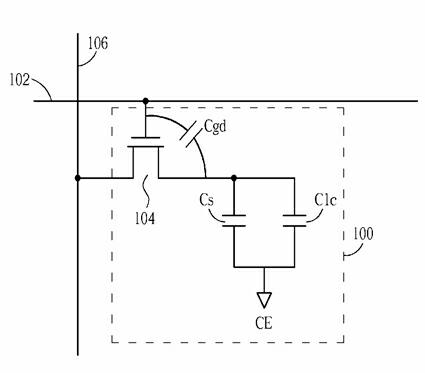
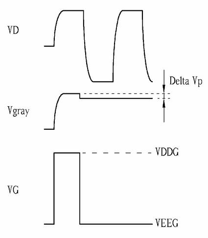
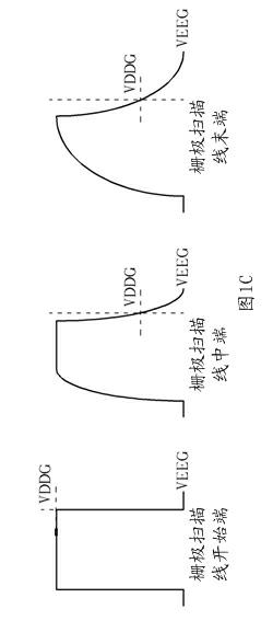
technical field [0001] The invention relates to a compensation circuit of a liquid crystal panel, in particular to a compensation circuit for improving the flicker phenomenon of the liquid crystal panel. Background technique [0002] Please refer to Figure 1A , Figure 1A It is a schematic diagram illustrating a pixel unit 100 in a liquid crystal panel in the prior art. When the thin-film transistor (thin-film transistor, TFT) 104 in the pixel unit 100 receives the control signal VG output by the gate scan line 102 as a high potential VDDG, the thin-film transistor 104 is turned on and the source scan line 106 is turned on according to the data voltage VD. The liquid crystal capacitor Clc in the pixel unit 100 is charged and discharged to a corresponding grayscale voltage Vgray. At this time, the gate potential of the thin film transistor 104 is the potential VDDG of the control signal VG. Additionally, if Figure 1A As shown, Cgd is the parasitic capacitance of the thin ...

Claims


Application Information

Patent Timeline
Patent Type & Authority Applications(China)
IPC IPC(8): G09G3/36
Inventor 蓝东鑫彭信渊赵世珩林锦宏
Owner 华映视讯(吴江)有限公司
Why Eureka
Eureka Blog
Learn More