
Imaging device, image processing method, image processing program and semiconductor integrated circuit

A camera device and image processing technology, applied in image data processing, image data processing, image enhancement, etc., can solve the problems of reducing the number of recorded pixels, shrinking RAW images, and processing redundant data, so as to maintain the maximum sense of resolution and prevent false positives. Signal, the effect of reducing false color

Active Publication Date: 2011-06-08
PANASONIC SEMICON SOLUTIONS CO LTD
View PDF4 Cites 2 Cited by
  • Summary
  • Abstract
  • Description
  • Claims
  • Application Information

AI Technical Summary

Problems solved by technology

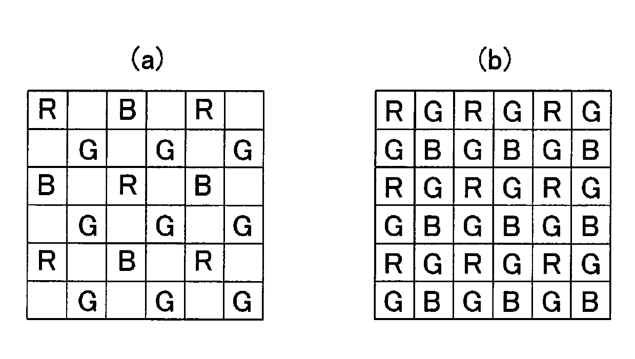
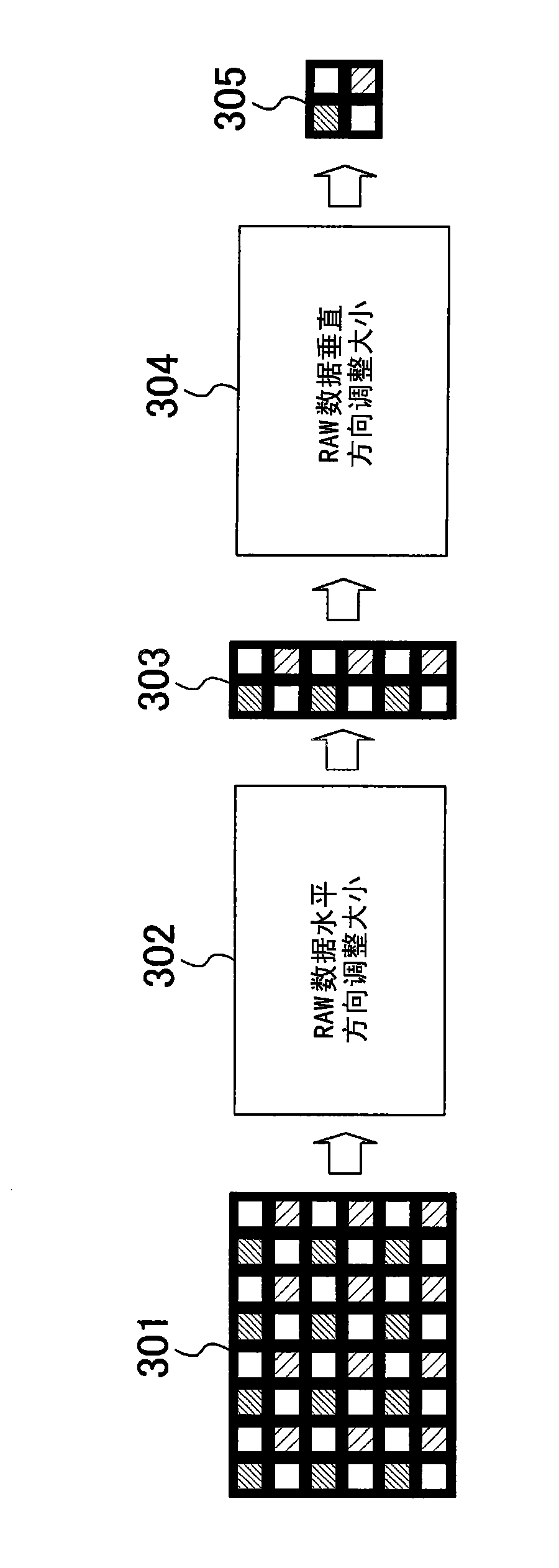
[0013] In the technologies of patent documents 1 to 3, when resizing the RAW data of RGB as the original image, color separation into independent R, G, and B data in the initial processing is adopted, or by mixing pixels of the same color The method of interval extraction, so when color separation is performed on the spatially configured RGB data in the RAW data, due to the interval extraction realized by sampling and pixel addition, it turns back to the high frequency near the low frequency Nyquist frequency Components cannot be removed by LPF, so high-frequency artifacts will be generated on the reduced RAW data that is reconfigured after reduction
As a result, false colors appear in the image, deterioration of the sense of resolution occurs, and there is a disadvantage that a reduced RAW image that fully utilizes the imaging characteristics of the original image cannot be obtained.
[0014] In addition, in the technology of Patent Document 4, the reduction and resizing process is performed after the image processing of the actual size, but the reduction and resizing process is a process of reducing the number of recording pixels, and the image processing is performed by thinning by the reduction and resizing process. The lost data becomes redundant processing, from the point of view of power saving, the efficiency is poor
Also, when it is installed in hardware such as LSI, since it is processed via an external memory buffer, the power consumption of the I / O buffer of the LSI is in proportion to the amount of processing.

Method used


Image

  • Imaging device, image processing method, image processing program and semiconductor integrated circuit
  • Imaging device, image processing method, image processing program and semiconductor integrated circuit
  • Imaging device, image processing method, image processing program and semiconductor integrated circuit

Examples


Embodiment Construction

[0040] Next, preferred embodiments of the image processing method and image processing program according to the present invention will be described in detail with reference to the drawings.

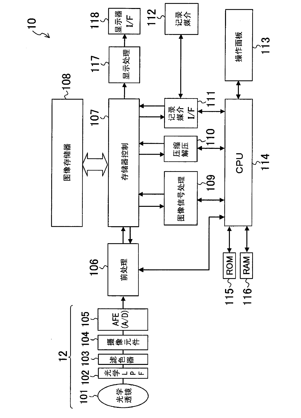
[0041] figure 1 It is a configuration diagram of the imaging device according to the embodiment of the present invention. This imaging device 10 is a single-board digital camera that converts an optical image of a subject captured by an imaging unit 12 into digital image data, and records the data on a recording medium 112 . The imaging unit 12 includes an optical lens 101 , an optical LPF 102 , a color filter 103 , an imaging element 104 , and an AFE (Analog Front End) unit 105 .

[0042] The imaging element 104 is an image sensor typified by a CCD type, a CMOS type, or the like. A plurality of photodiodes (light-sensitive pixels) are two-dimensionally arranged on the light-receiving surface of the imaging element 104 , and photoelectrically converts object information passing through ...


PUM


Abstract

The invention provides an imaging device, an image processing method, an image processing program and a semiconductor integrated circuit. After the brightness data and the color carrier data are extracted by filter processes (602, 606) in line units without separating the colors of the original image, namely, the CCDRAW image (601), obtained from the single color imaging element into R, G, B datacorresponding to the Bayer matrix, and a color difference data demodulation process (607) and a median noise removal process (608) are applied to the color carrier data, bandlimiting filter processes(603, 609) having different characteristics are applied to the brightness data and the color difference data. Furthermore, resize processes (604, 610) are independently performed for the brightness data and the color difference data. The color carrier data from the resized color difference data are passed through a modulation process (611), and a color matrix reproduction process (612) which involves recombining the color carrier data and the resized brightness signal is executed.

Description

technical field [0001] The present invention relates to an imaging device, an image processing method, an image processing program, and a semiconductor integrated circuit equipped with an image processing function, and in particular to an image suitable for reduction processing, enlargement processing, and deformation correction of an original image obtained from a single-board color imaging element Data size conversion processing device, electronic still picture camera, image data size conversion processing program, semiconductor integrated circuit, etc. Background technique [0002] There is known a digital camera that captures an image of a subject passing through a photographic lens with an imaging element such as a CCD or a MOS sensor, and then performs predetermined image processing on image data output from the imaging element. A general digital camera converts the image signal obtained from the imaging element into 10-bit, 12-bit, or 14-bit digital data, performs var...

Claims


Application Information

Patent Timeline
Patent Type & Authority Applications(China)
IPC IPC(8): H04N9/07G06T1/00G06T3/40H04N1/393H04N1/46H04N23/12H04N23/40
CPCH04N1/56G06T3/40H04N1/393G06T3/4015H04N9/045G06T5/002G06T5/006G06T2200/12G06T5/001H04N1/46G06T2207/10024H04N23/843H04N25/134G06T5/80G06T5/70
Inventor 秦野敏信
Owner PANASONIC SEMICON SOLUTIONS CO LTD
Learn More