

Touch display panel
A technology for touching the display panel and the display area, which is applied to the input/output process of instruments, electrical digital data processing, and data processing, etc. Effects of interference and parasitic capacitance suppression
Inactive Publication Date: 2011-06-15
AU OPTRONICS CORP
View PDF3 Cites 29 Cited by
- Summary
- Abstract
- Description
- Claims
- Application Information
AI Technical Summary
Problems solved by technology
However, since the display panel itself is also a source of signal generation, especially the distance between the sensing series of the touch panel and the electrode layer of the display panel is relatively close, a larger parasitic capacitance is likely to be generated.
In this way, the sensing signal received by the touch panel will be seriously interfered, which will lead to the problem of lowering the sensing sensitivity (sensitivity)
Method used
View moreImage
Smart ImageViewing Examples

Examples
Embodiment Construction
Login to View More PUM
 Abstract
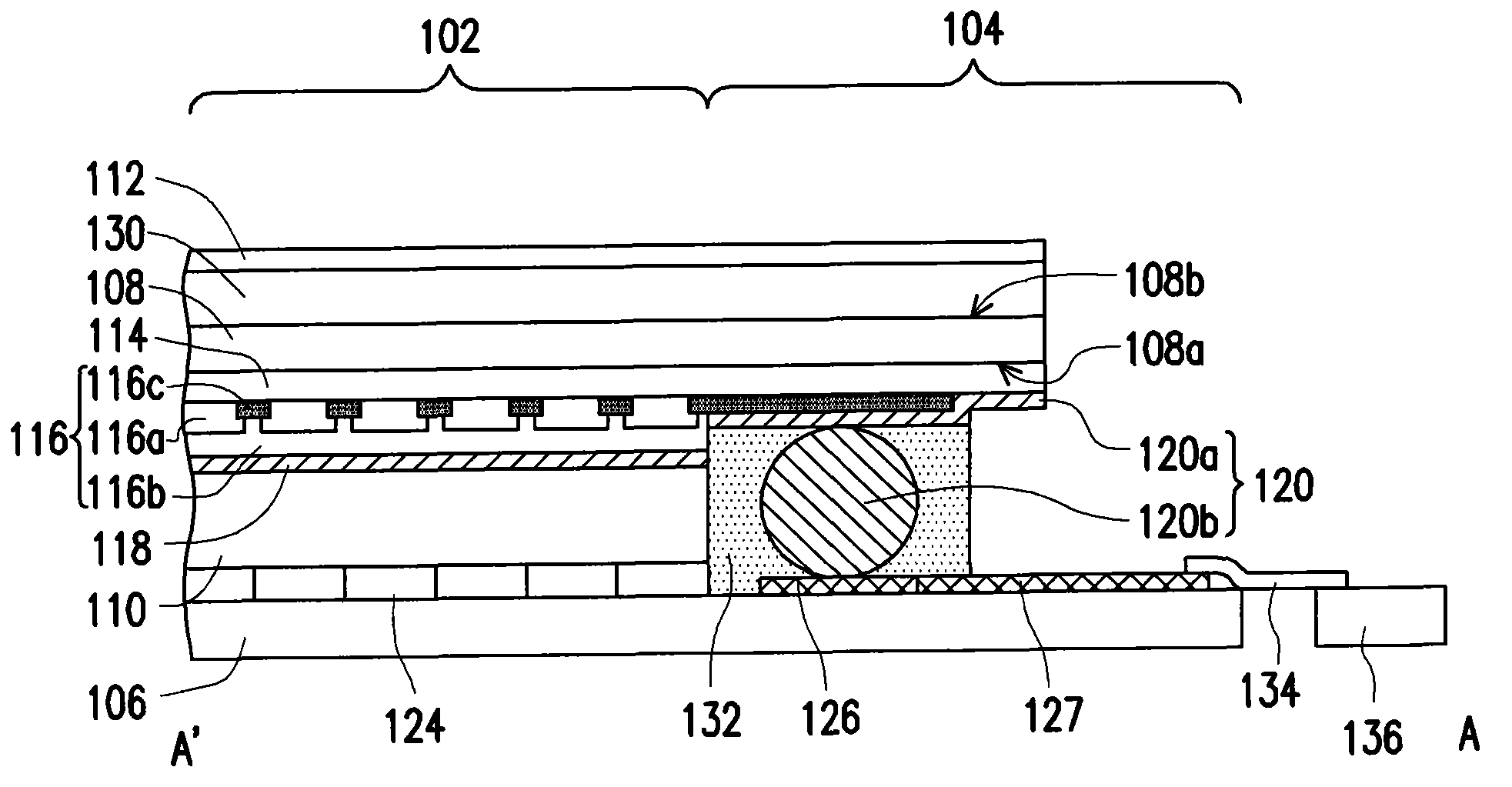
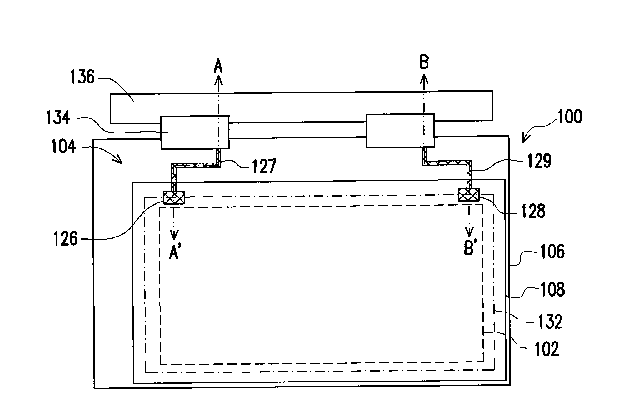
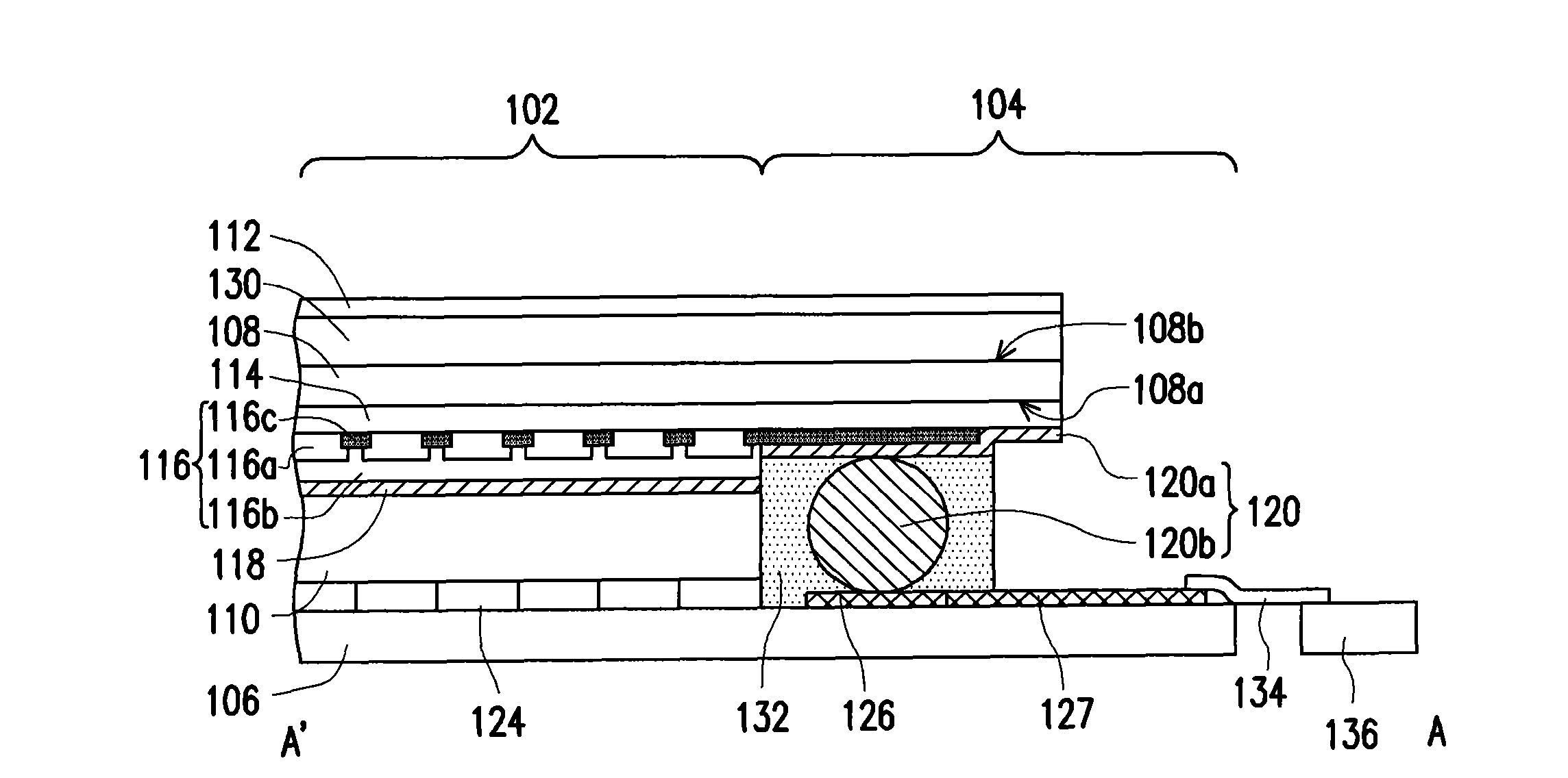
Provided is a touch display panel, comprising a first substrate, a second substrate, a display medium layer, a touch induction component, a shielding conductive layer, an insulating layer, an electrode layer, a first conducting structure and a second conducting structure. The first substrate is provided with a plurality of pixel structures in a display region and with a first pad and a second pad in a peripheral region. The first and the second pads are electrically connected to a first and second potentials respectively. The display medium layer is disposed between the first substrate and the second substrate. The touch induction component is disposed on the outer surface of the second substrate. The shielding conductive layer is arranged on the inner surface of the second substrate. The insulating layer and the electrode layer are arranged on the shielding conductive layer in order, facing towards the first substrate. The first conducting structure lies in the peripheral region and makes the shielding conductive layer be electrically connected to the first pad. The second conducting structure lies in the peripheral region and makes the electrode layer be electrically connected to the second pad.
Description
touch display panel technical field The present invention relates to a touch-sensing display panel, and in particular to a capacitive touch display panel. Background technique With the advancement of display technology, people can make their lives more convenient with the assistance of displays. In order to achieve the characteristics of lightness and thinness of displays, flat panel displays (FPDs) have become the current mainstream. In recent years, all kinds of electronic products are constantly moving towards the direction of easy operation, small size and large screen size, especially portable electronic products have stricter requirements on volume and screen size. Therefore, many electronic products integrate the touch-sensitive design with the display panel, so as to omit the space required for the keyboard or control buttons, thereby expanding the configurable area of the screen. Generally speaking, the touch display panel includes a display panel and a touch ...
Claims
Login to View More Application Information
Patent Timeline
 Patent Type & Authority Applications(China)
IPC IPC(8): G06F3/041G06F3/044
Inventor 林建宏郭文瑞童腾赋庄堇桦
Owner AU OPTRONICS CORP