Method for manufacturing semiconductor device having multi-layered contact

a semiconductor device and multi-layered technology, applied in the direction of semiconductor devices, basic electric elements, electrical appliances, etc., can solve the problems of increasing error, increasing contact resistance, and reducing the efficiency of the device isolation region, so as to achieve the effect of suppressing the parasitic capacitance encountered between neighboring bit lines

Active Publication Date: 2012-10-30
SK HYNIX INC
View PDF14 Cites 10 Cited by
  • Summary
  • Abstract
  • Description
  • Claims
  • Application Information

AI Technical Summary

Benefits of technology

[0010]An embodiment of the present invention relates to a method for manufacturing a semiconductor device in which a metal line coupled to a transistor constructing a sense amplifier (sense-amp) is formed of two layers, so that a step difference between the metal line and the bit line of the cell region can be reduced and parasitic capacitance encountered between neighbor bit lines can be suppressed.

Problems solved by technology

As a design rule is reduced to 100 nm or less so as to increase the integration degree of the semiconductor memory device, a cross-sectional area occupied by constituent elements of the semiconductor memory device is reduced, resulting in various problems.
When forming a contact, an alignment error is increased so that contact resistance is also increased.
For example, in a fabrication process of 40 nm or less in an 8F2 structure, a process for forming a device isolation region defining the active region is also becoming difficult.
In addition, as the width of a gate pattern is gradually reduced, an aspect ratio of the gate pattern is increased, resulting in a defect such as an inclined part.
In addition, from the viewpoint of a gate pattern, if the overlap degree is reduced because of an alignment error encountered between a recess region formed when a trench formed in an active region is buried and a pattern formed over the active region occurs, there arise various problems (for example, increase in resistance, reduction in fabrication margin for contact formation, etc.).
In fact, as the space is gradually reduced in width, it is more difficult to form a pattern as well as to form a contact hole for forming a contact.
As a result, parasitic capacitance is unavoidably increased such that the reliability of the semiconductor device is reduced.
Due to the step difference between the cell region and the core and peripheral region, it may be difficult to form a wiring for coupling constituent elements contained in the cell region to constituent elements contained in the core and peripheral region.
Therefore, provided that a step difference between the cell region and the core region is high, there is a high probability that a bit line is severed due to the high step difference.
As described above, according to the method for manufacturing conventional semiconductor devices, under a current design rule, the parasitic capacitance between metal lines is increased and the fabrication tolerances are unavoidably reduced because it is difficult to form a metal line due to a difference in height (i.e., a step difference) between the cell region and the core and peripheral region.
Specifically, the increase in parasitic capacitance of a bit line for coupling a cell transistor to a sense amplifier (sense-amp) and the reduction in fabrication tolerances may have a negative influence upon the operation characteristics of the sense amplifier.

Method used


Image

  • Method for manufacturing semiconductor device having multi-layered contact
  • Method for manufacturing semiconductor device having multi-layered contact
  • Method for manufacturing semiconductor device having multi-layered contact

Examples


Embodiment Construction

[0026]Reference will now be made in detail to embodiments of the present invention, examples of which are illustrated in the accompanying drawings. Wherever possible, the same reference numbers will be used throughout the drawings to refer to the same or like parts.

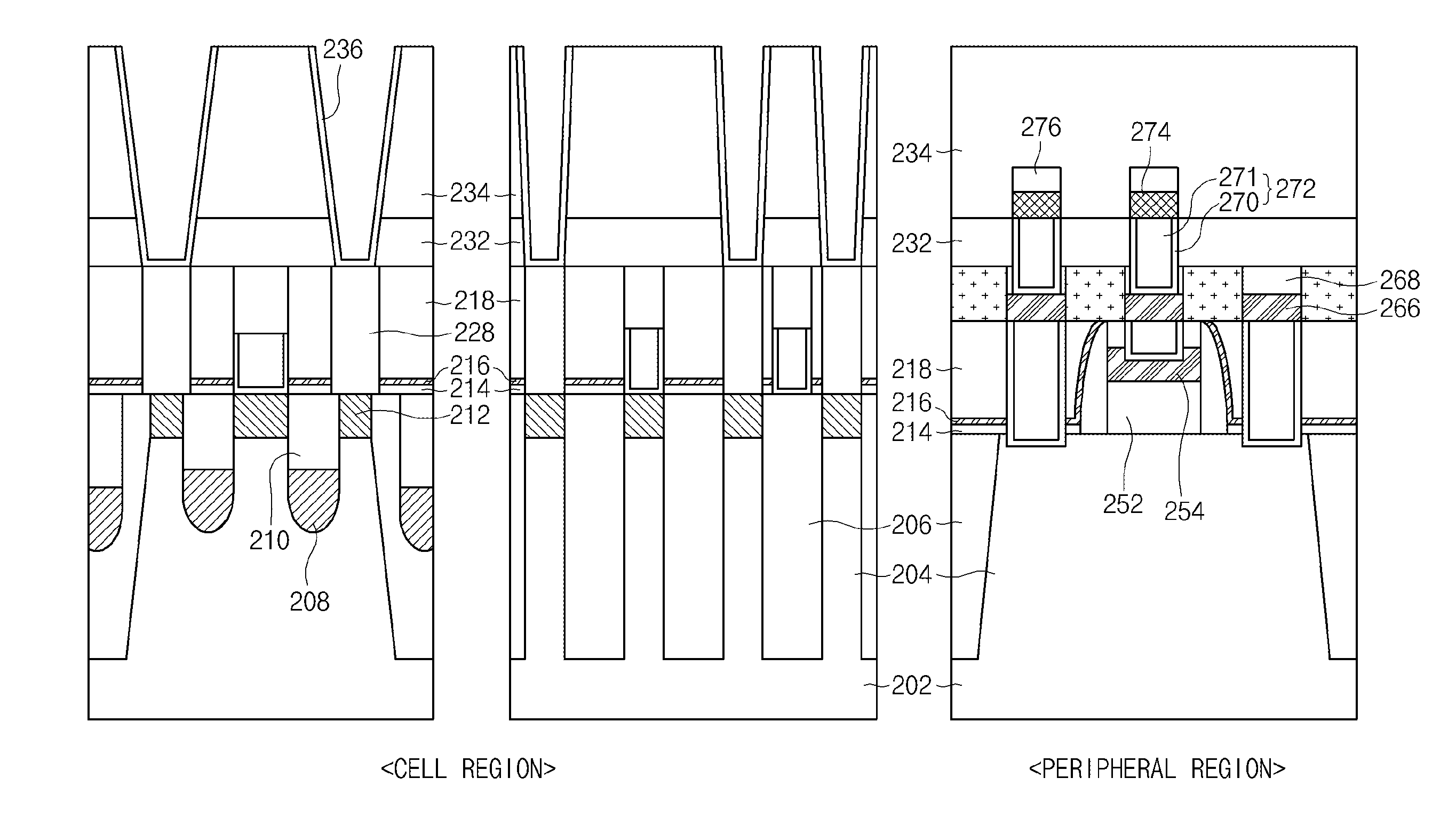
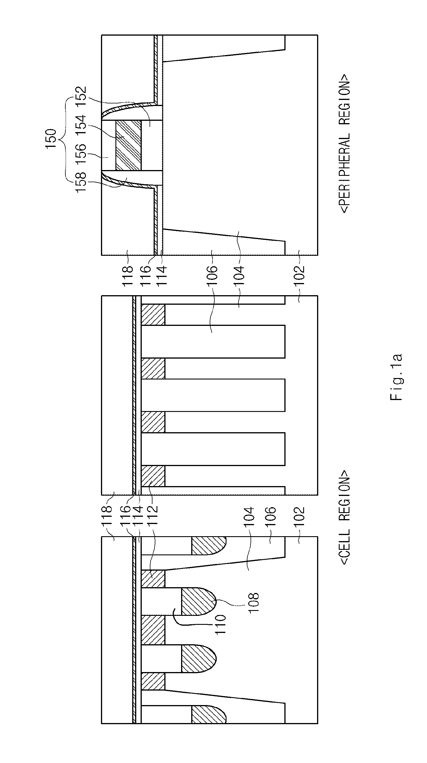
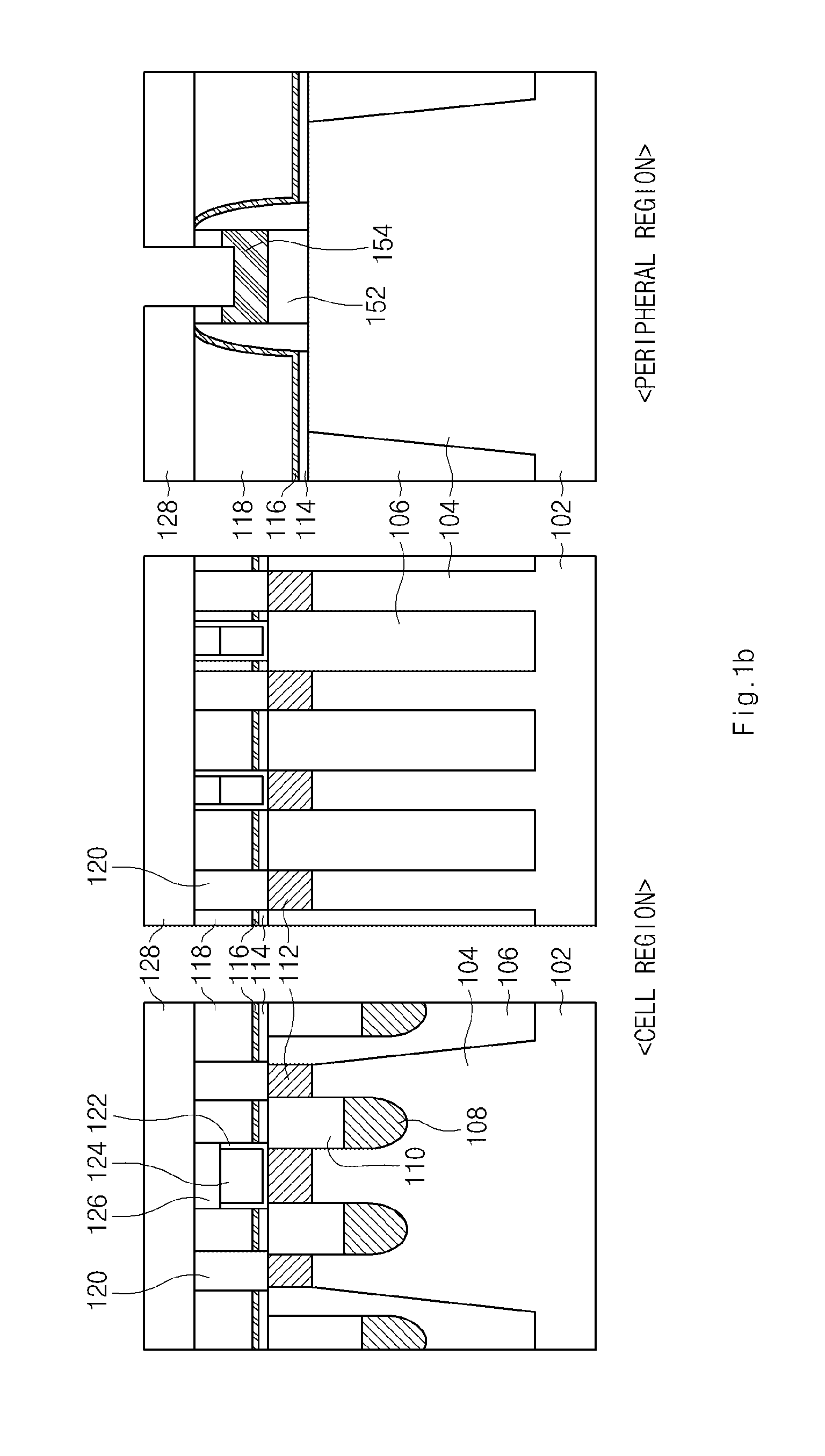
[0027]Embodiments of the present invention relate to a technology for increasing the reliability of a semiconductor device. In particular, the embodiments of the present invention relate to a method for manufacturing a semiconductor device, which can minimize a step difference between the cell region and the core and peripheral region (hereinafter referred to as ‘peripheral region’) when forming a metal line for coupling constituent elements of the cell region to those of the peripheral region.

[0028]A method for manufacturing a semiconductor device according to the embodiments of the present invention will hereinafter be described with reference to the drawings.

[0029]FIGS. 1A to 1D are cross-sectional views illustrating a...


PUM


Abstract

A method for manufacturing a semiconductor device is disclosed, which reduces a step difference between a peripheral region and a cell region. In the semiconductor device, a metal contact of the peripheral region is configured in a multi-layered structure. Prior to forming a bit line and a storage node contact in the cell region, a contact and a line are formed in the peripheral region, such that a step difference between the cell region and the peripheral region is reduced, resulting in a reduction in parasitic capacitance between lines.

Description

CROSS-REFERENCE TO RELATED APPLICATION[0001]The priority of Korean patent application No. 10-2010-0119204 filed on Nov. 26, 2010, the disclosure of which is hereby incorporated in its entirety by reference, is claimed.BACKGROUND OF THE INVENTION[0002]Embodiments of the present invention relate to a method for manufacturing a highly-integrated semiconductor device, and more particularly to a method for manufacturing a semiconductor device to suppress parasitic capacitance between metal lines contained in a highly-integrated semiconductor device, such that the reliability of the semiconductor device is increased.[0003]Generally, a semiconductor is a material that belongs to an intermediate region between a conductor and an insulator. Although the semiconductor is similar to an insulator in a pure state, electrical conductivity of the semiconductor device is increased by impurity implantation or other manipulation. The semiconductor is used to form a semiconductor device such as a tran...

Claims


Application Information

Patent Timeline
Patent Type & Authority Patents(United States)
IPC IPC(8): H01L21/336
CPCH01L27/10894H01L27/10897H01L27/10876H01L27/10885H10B12/50H10B12/053H10B12/482H10B12/09
Inventor KIM, JUNG NAM
Owner SK HYNIX INC
Why Eureka
Try Eureka