Display device with touch detection function and electronic apparatus

a technology of touch detection and electronic equipment, which is applied in the direction of electric digital data processing, instruments, computing, etc., can solve the problems of longer time for charging and discharging the drive electrode, and achieve the effects of reducing the size of the driver ics, suppressing parasitic capacitance, and suppressing the power consumption of touch detection

Active Publication Date: 2017-11-02
JAPAN DISPLAY INC
View PDF11 Cites 9 Cited by
  • Summary
  • Abstract
  • Description
  • Claims
  • Application Information

AI Technical Summary

Benefits of technology

[0110]As describe above, suppressing the parasitic capacitance between the drive electrodes COML and the pixel signal lines SGL allows the display device with a touch detection function 1 to suppress the power consumption of the touch detection. This, in turn, can suppress the power supplied to the touch detection unit 40, leading to a possible reduction in the size of driver ICs. This can reduce the size of an electronic apparatus including the display device with a touch detection function 1 of the first embodiment.
[0111]The suppression of the parasitic capacitance between the drive electrodes COML and the pixel signal lines SGL also allows the display device with a touch detection function 1 according to the first embodiment to suppress the influence on charging and discharging. This allows the frequency of the rectangular wave of the touch drive signal Vcomt to be increased. This, in turn, results in suppression of an influence of low-frequency noise caused by an AC power supply in the display device with a touch detection function 1 according to the first embodiment. The display device with a touch detection function 1 according to the first embodiment can increase the frequency of the rectangular waves of the touch drive signals Vcomt supplied to the drive electrodes COML, and thus can perform the touch detection in a short time. This allows the display device with a touch detection function 1 according to the first embodiment to cope with an increase in screen area or definition of the touch detection device 30. The display device with a touch detection function 1 according to the first embodiment can reduce the parasitic capacitance between the drive electrodes COML and the pixel signal lines SGL even when the distance between the drive electrodes COML and the pixel signal lines SGL is reduced, and thus can reduce the thickness of the display unit with a touch detection function 10.
[0112]FIG. 16 is a schematic diagram explaining a relation among the drive electrodes, the pixel signal lines, and the pixels in a module implemented with a display device with a touch detection function according to a modification of the first embodiment. As described above, while the drive electrodes COML are transparent, the gaps between the adjacent drive electrodes COML are likely to be noticed as stripes by human eyes. For this reason, in this display device with a touch detection function 1 according to the modification of the first embodiment, the gap between the adjacent drive electrodes COML is positioned between the color region 32R of red (R) and the color region 32B of blue (B) whose brightnesses are relatively low. This can reduce the aperture ratio of the color region 32R of red (R) and the color region 32B of blue (B). For example, in the display device with a touch detection function 1 according to the modification of the first embodiment, as illustrated in FIG. 16, the length between the pixel signal lines SGL each lying between the color region 32R of red (R) and the color region 32B of blue (B) is denoted as Ls, and the length of the width of the drive electrode COML orthogonal to the extending direction thereof is denoted as Lc. In the display device with a touch detection function 1 according to the modification of the first embodiment, as illustrated in FIG. 16, the pixel signal lines SGL are arranged with the sub-pixels SPix illustrated in FIG. 10 interposed therebetween, the sub-pixels SPix overlapping the red color region 32R of red (R), the green color region 32G of green (G), and the blue color region 32B of blue (B) of the color filter 32 when viewed in the direction orthogonal to the surface of the TFT substrate 21 as described above. The lengths between the pixel signal lines SGL thus arranged are denoted as a width Δr, a width Δg, and a width Δb.
[0113]The gap between the adjacent drive electrodes COML is positioned between the color region 32R of red (R) and the color region 32B of blue (B) whose brightnesses are relatively low. This maintains the aperture ratio of the color region 32G of green (G) having a higher brightness than those of the color region 32R of red (R) and the color region 32B of blue (B). Making the widths Δr and Δb larger than the width Δg can increase the aperture ratios of the color region 32R of red (R) and the color region 32B of blue (B). In the display device with a touch detection function 1 according to the modification of the first embodiment, the color region 32R of red (R) and the color region 32B of blue (B) of the color filter 32 are arranged with the color region 32G of green (G) interposed therebetween, and the width of each of the color region 32R of red (R) and the color region 32B of blue (B) in a direction orthogonal to the extending direction thereof is smaller than the width of the color region 32G of green (G) in a direction orthogonal to the extending direction thereof. This can equalize transmittance values of the color regions 32R, 32G, and 32B of the color filter 32 colored in the three colors of red (R), green (G), and blue (B) in the display device with a touch detection function 1 according to the modification of the first embodiment. For example, each of the widths Δr and Δb can be larger than the width Δg by approximately [(length Ls−length Lc) / 2].
[0114]In the display device with a touch detection function 1 according to the modification of the first embodiment, the length of the gap between the adjacent drive electrodes COML is periodically arranged on a pixel Pix by pixel Pix basis. This reduces the possibility that the person notices the stripes associated with the gaps between the adjacent drive electrodes COML.
[0115]A display device with a touch detection function 1 according to a second embodiment of the present disclosure will be described. FIG. 17 is a schematic diagram of a cross section, explaining a relation among the drive electrodes, the pixel signal lines, and the pixel electrodes in a module implemented with the display device with a touch detection function according to the second embodiment. FIG. 18 is a schematic diagram explaining a relation among the drive electrodes, the pixel signal lines, and the pixels in the module implemented with the display device with a touch detection function according to the second embodiment. The same constituent elements as those described in the first embodiment above will be given the same numerals, and duplicate description thereof will be omitted.

Problems solved by technology

When the drive electrode and the signal line three-dimensionally cross each other, a larger parasitic capacitance is produced between the drive electrode and the signal line, so that charging and discharging the drive electrode takes a longer time.

Method used


Image

  • Display device with touch detection function and electronic apparatus
  • Display device with touch detection function and electronic apparatus
  • Display device with touch detection function and electronic apparatus

Examples


first embodiment

1-1. First Embodiment

1-1A. Configuration Examples

Overall Configuration Example

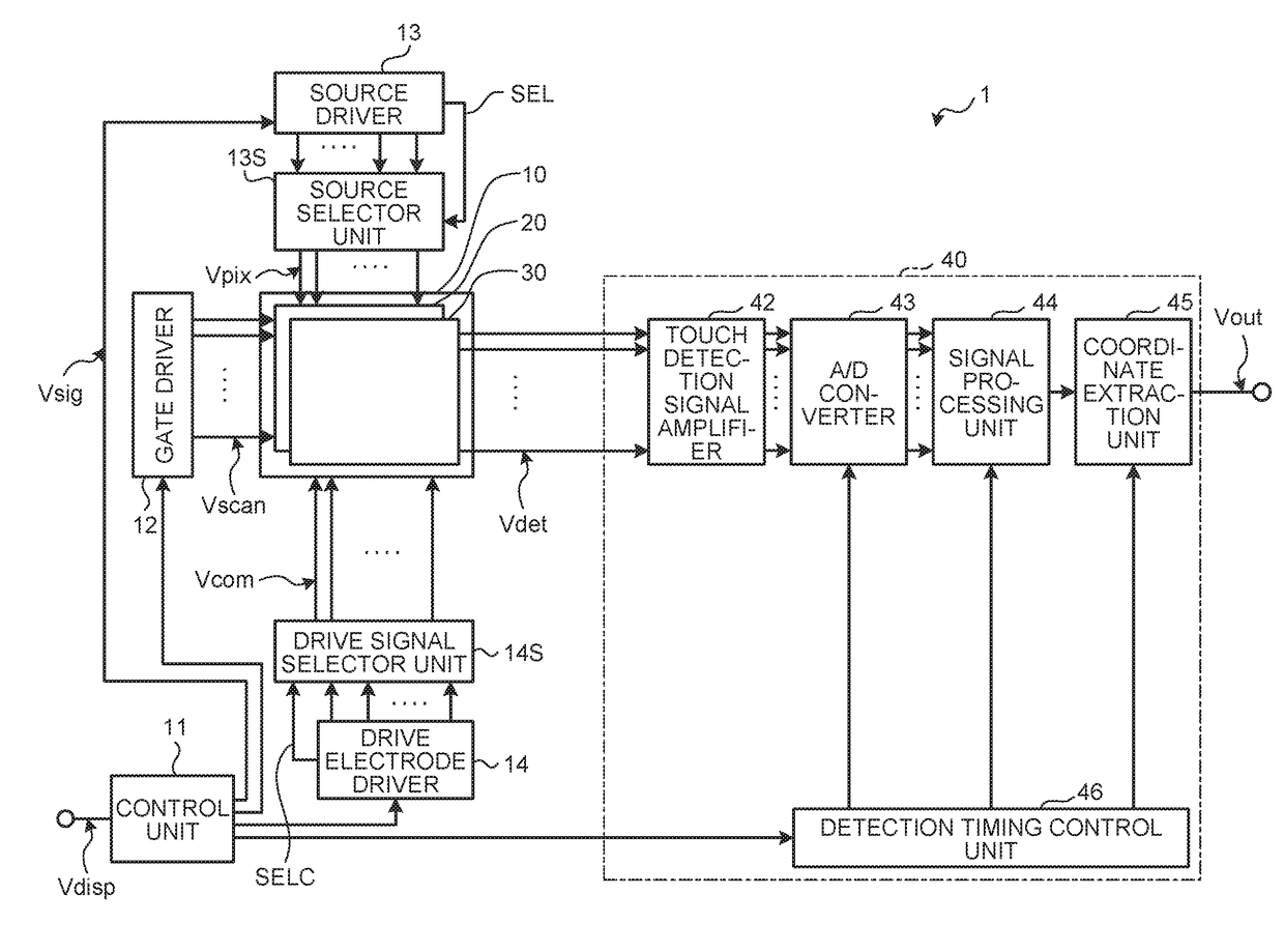
[0056]FIG. 1 is a block diagram illustrating a configuration example of a display device with a touch detection function according to a first embodiment of the present disclosure. This display device with a touch detection function 1 includes a display unit with a touch detection function 10, a control unit 11, a gate driver 12, a source driver 13, a source selector unit 13S, a drive electrode driver 14, a drive signal selector unit 14S, and a touch detection unit 40. The display device with a touch detection function 1 is a display device in which the display unit with a touch detection function 10 has a built-in touch detection function. The display unit with a touch detection function 10 is what is called an in-cell type device obtained by integrating a liquid-crystal display unit 20 using liquid-crystal display elements as display elements with an electrostatic capacitance type touch detection device 3...

second embodiment

1-2A. Modification of Second Embodiment

[0119]FIG. 19 is a schematic diagram of a cross section, explaining a relation among the drive electrodes, the pixel signal lines, and the pixel electrodes in a module implemented with a display device with a touch detection function according to a modification of the second embodiment. FIG. 20 is a schematic diagram explaining a relation among the drive electrodes, the pixel signal lines, and the pixels in the module implemented with the display device with a touch detection function according to the modification of the second embodiment. The same constituent elements as those described in the first embodiment above will be given the same numerals, and duplicate description thereof will be omitted.

[0120]As illustrated in FIG. 19, the drive electrodes COML face the pixel electrodes 22 in the direction orthogonal to the surface of the TFT substrate 21. As illustrated in FIGS. 19 and 20, each one of the drive electrodes COML is arranged so as to ...

third embodiment

1-3. Third Embodiment

[0125]A display device with a touch detection function 1A according to a third embodiment of the present disclosure will be described. FIG. 21 is a diagram illustrating an example of a module implemented with the display device with a touch detection function according to the third embodiment. FIG. 22 is a schematic diagram explaining a relation between the drive electrodes and the pixel signal lines in the module implemented with the display device with a touch detection function according to the third embodiment. The same constituent elements as those described in the first embodiment or the second embodiment above will be given the same numerals, and duplicate description thereof will be omitted.

[0126]FIG. 21 schematically illustrates, in the direction orthogonal to the surface of the TFT substrate 21 described above, the display unit with a touch detection function 10 having the drive electrodes COML, and the scan signal lines GCL that are formed so as to th...


PUM


Abstract

According to an aspect, a display device with a touch detection function includes a plurality of drive electrodes that face a plurality of pixel electrodes in an orthogonal direction to the surface of the substrate, and extend in a direction parallel to the direction in which a plurality of signal lines extend. The display device with a touch detection function also includes a scan driving unit that applies a touch drive signal to a signal line that faces, in an overlapping manner in the orthogonal direction, a drive electrode to which the touch drive signal is applied.

Description

CROSS-REFERENCE TO RELATED APPLICATIONS[0001]The present application is a continuation of U.S. patent application Ser. No. 15 / 248,239, filed on Aug. 26, 2016, which application is a continuation of U.S. patent application Ser. No. 14 / 918,851, filed on Oct. 21, 2015, issued as U.S. Pat. No. 9,442,596 on Sep. 13, 2016, which is a continuation of U.S. patent application Ser. No. 14 / 098,132, filed Dec. 5, 2013, issued as U.S. Pat. No. 9,201,541, on Dec. 1, 2015, which claims priority to Japanese Application No. 2012-266784, filed Dec. 5, 2012, and claims priority to Japanese Application No. 2013-251696, filed Dec. 5, 2013, the entire contents of which are hereby incorporated herein by reference.BACKGROUND1. Technical Field[0002]The present disclosure relates to a display device and an electronic apparatus that can detect an external proximity object, and particularly to a display device with a touch detection function and an electronic apparatus that can detect an external proximity obj...

Claims


Application Information

Patent Timeline
Patent Type & Authority Applications(United States)
IPC IPC(8): G06F3/044G06F3/041
CPCG06F3/0416G06F3/0412G06F3/044G06F3/0418G06F3/04166G06F3/04182G06F3/0446
Inventor KIDA, YOSHITOSHINOGUCHI, KOJITERANISHI, YASUYUKIMIZUHASHI, HIROSHIAZUMI, KOHEI
Owner JAPAN DISPLAY INC
Why Eureka
Try Eureka