Plasma display device, and method for driving plasma display panel

A technology for display devices and display panels, which is applied to static indicators, instruments, etc., and can solve problems such as image display quality degradation

Inactive Publication Date: 2011-06-29
PANASONIC CORP
View PDF2 Cites 0 Cited by
  • Summary
  • Abstract
  • Description
  • Claims
  • Application Information

AI Technical Summary

Problems solved by technology

Such erroneous discharge causes image display quality to deteriorate

Method used


Image

  • Plasma display device, and method for driving plasma display panel
  • Plasma display device, and method for driving plasma display panel
  • Plasma display device, and method for driving plasma display panel

Examples


Embodiment approach 1

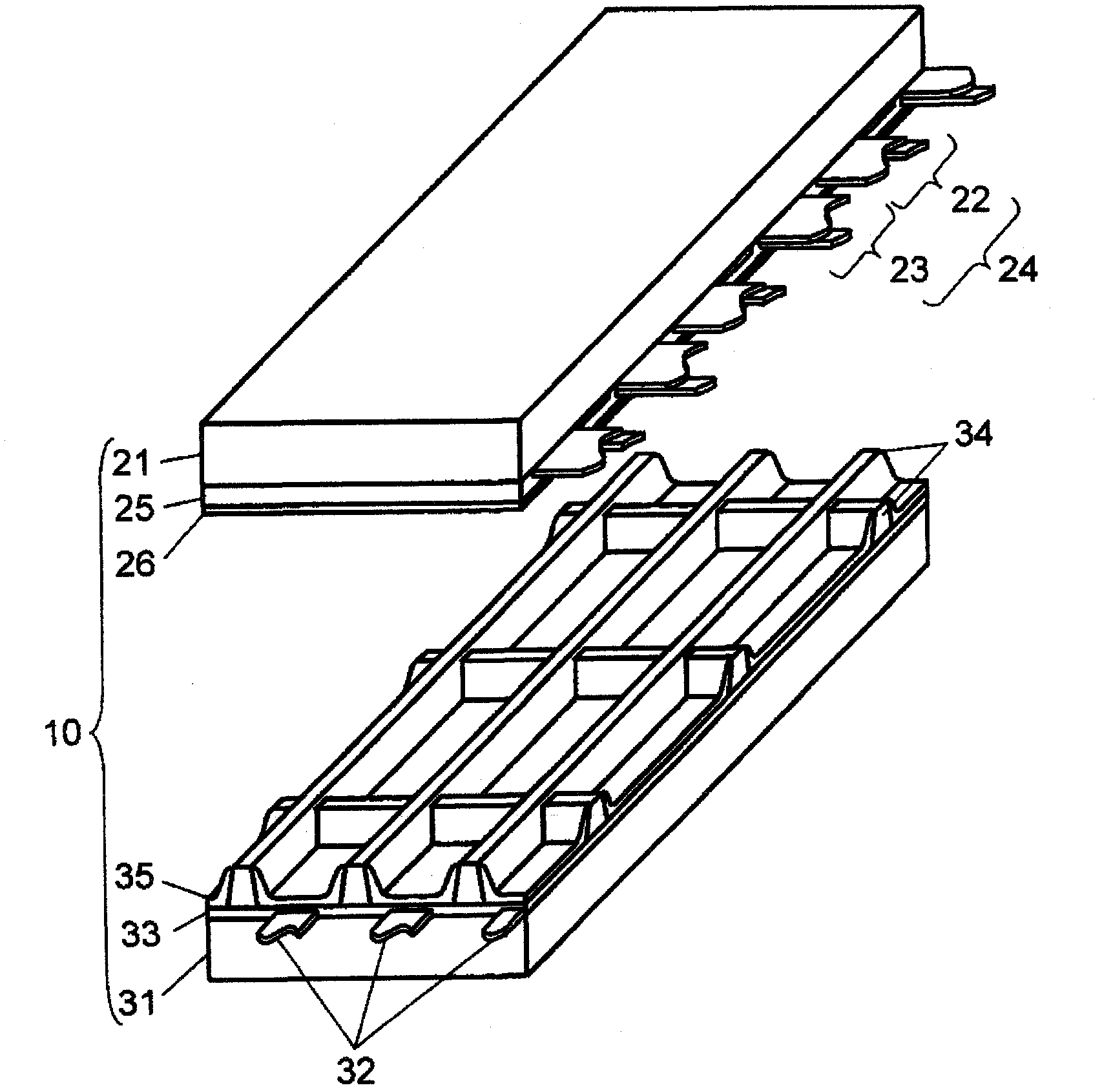
[0036] figure 1 It is an exploded perspective view showing the structure of the panel 10 according to Embodiment 1 of the present invention. On front panel 21 made of glass, a plurality of display electrode pairs 24 including scan electrodes 22 and sustain electrodes 23 are formed. Furthermore, dielectric layer 25 is formed to cover scan electrodes 22 and sustain electrodes 23 , and protective layer 26 is formed on dielectric layer 25 .

[0037] In addition, in order to reduce the discharge start voltage in the discharge cell, the protective layer 26 is formed of a material mainly composed of MgO that is actually used as a panel material. When MgO is sealed with neon (Ne) and xenon (Xe) gases, The secondary electron emission coefficient is large, and the durability is good.

[0038] A plurality of data electrodes 32 are formed on the rear panel 31 . Furthermore, dielectric layer 33 is formed so as to cover data electrode 32 . Furthermore, a grid-shaped spacer 34 is further...

Embodiment approach 2

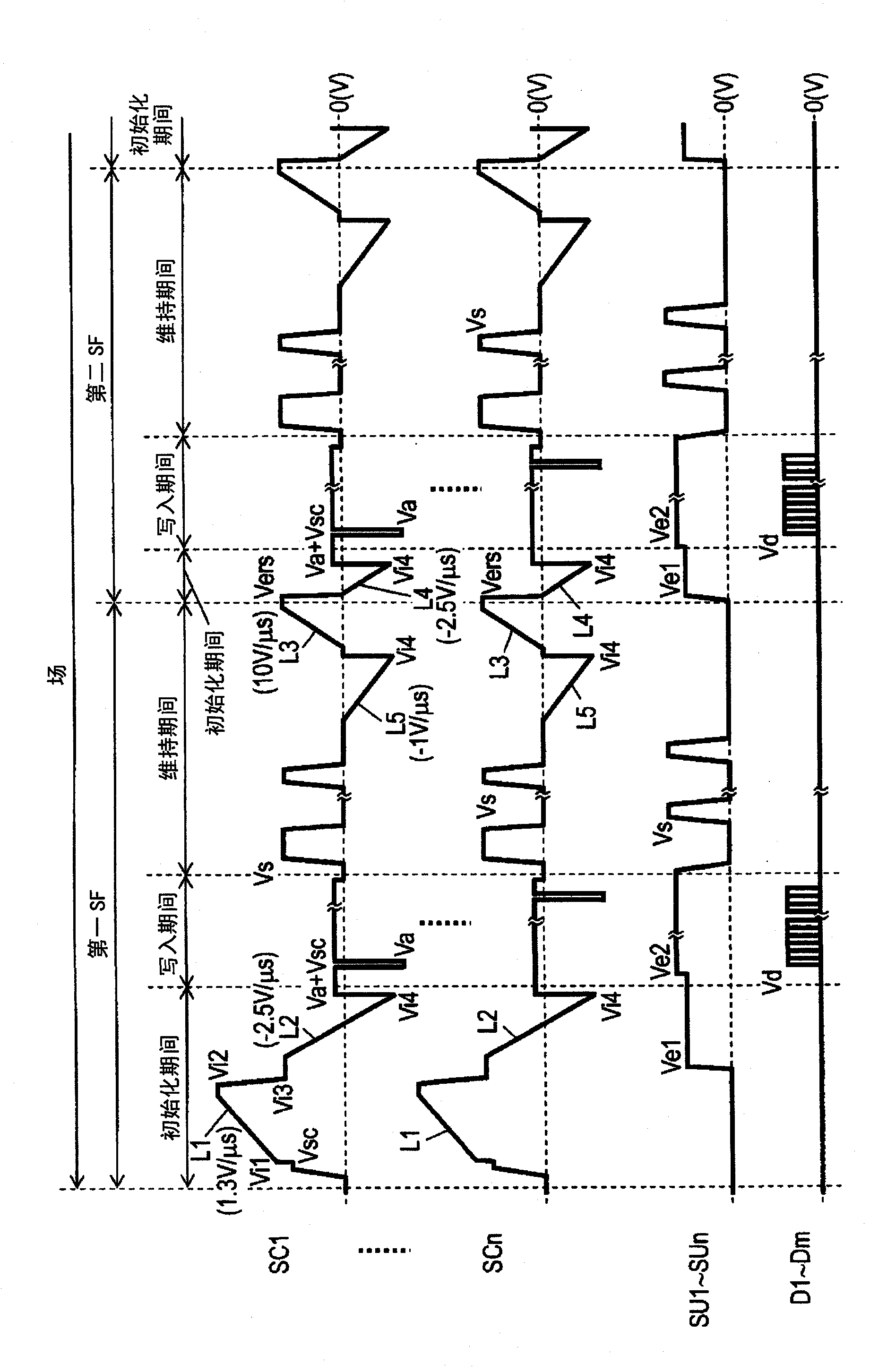
[0147] In Embodiment 1, an example has been described in which the cancel down-ramp voltage L5 is generated in a waveform shape with a gentler slope than the down-ramp voltage L2 and the down-ramp voltage L4 . However, in the present invention, the waveform shape of the erasing down ramp voltage is not limited to any waveform shape of the erasing down ramp voltage L5. In this embodiment, an example in which the erasing down-ramp voltage is generated in a waveform shape different from that of the erasing down-ramp voltage L5 will be described.

[0148] Figure 10 It is a driving voltage waveform chart applied to each electrode of panel 10 in Embodiment 2 of this invention. In addition, in this embodiment, the erasing down-ramp voltage shown in this embodiment is called "eliminating down-ramp voltage L6". In addition, in this embodiment, in the driving voltage waveform applied to scan electrode SC1 -scan electrode SCn, erasing down ramp voltage L6 is used instead of erasing do...


PUM


Abstract

In a highly definition plasma display panel, wall charges are properly adjusted to perform writing operations stably, and the generation of an abnormal discharge for a write period is suppressed to improve the quality of image display. Provided is a plasma display device comprising a plasma display panel having a plurality of scanning electrodes, and a scanning electrode drive circuit for generating a falling ramp voltage (L2) or a falling ramp voltage (L4), which is a first descending voltage falling for an initialization period, generating a maintaining pulse for a maintenance period, and generating a rising erasure ramp voltage (L3), which is an ascending voltage rising finally of the maintenance period, thereby to apply same to the scanning electrodes. The scanning electrode drive circuit generates, after the generation of the maintenance pulse for the maintenance period, a falling erasure ramp voltage (L5), i.e., a second descending voltage having portions descending at a gentler gradient than those of the falling ramp voltage (L2) and the falling ramp voltage (L4), and generates the rising erasure ramp voltage (L3) after the generation of the falling erasure ramp voltage (L5), and applies same to the scanning electrodes.

Description

technical field [0001] The invention relates to a plasma display device and a driving method for a wall-mounted television or a large monitor and a plasma display panel. Background technique [0002] A typical AC surface discharge panel, which is a plasma display panel (hereinafter abbreviated as "panel"), has a large number of discharge cells formed between a front panel and a rear panel facing each other. In the front panel, a plurality of display electrode pairs consisting of a pair of scan electrodes and a pair of sustain electrodes are formed parallel to each other on the front glass substrate. And, a dielectric layer and a protective layer are formed to cover these display electrode pairs. In the rear plate, a plurality of parallel data electrodes are formed on a rear glass substrate, a dielectric layer is formed to cover these data electrodes, and a plurality of barrier ribs are formed on these in parallel to the data electrodes. In addition, phosphor layers are for...

Claims


Application Information

Patent Timeline
Patent Type & Authority Applications(China)
IPC IPC(8): G09G3/28G09G3/20G09G3/288G09G3/291G09G3/292G09G3/294G09G3/296G09G3/298
CPCG09G2310/066G09G3/2927G09G3/296G09G3/291
Inventor 富冈直之野口直树
Owner PANASONIC CORP
Why Eureka
Try Eureka