
Optical zoom system

An optical zoom and optical lens technology, applied in the field of optical systems, can solve the problems that the volume of the optical zoom system cannot be effectively reduced, it is difficult to achieve volume miniaturization, etc., and achieve the best optical imaging quality, small overall volume, and reduced overall volume. Effect

Inactive Publication Date: 2014-05-14
HIMAX TECH LTD
View PDF2 Cites 0 Cited by
  • Summary
  • Abstract
  • Description
  • Claims
  • Application Information

AI Technical Summary

Problems solved by technology

[0005] Because the optical lens 120 is located in the focus motor 130, and the focus motor 130 is fitted with the optical lens 120 through the telescopic structure 132 to control the action of the optical lens 120 approaching or moving away from the light sensor 110, but with such a structure, the The overall volume of the optical zoom system 100 cannot be effectively reduced, and it is difficult to achieve the purpose of volume miniaturization

Method used


Image

  • Optical zoom system
  • Optical zoom system
  • Optical zoom system

Examples


Embodiment Construction

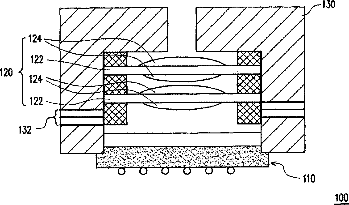
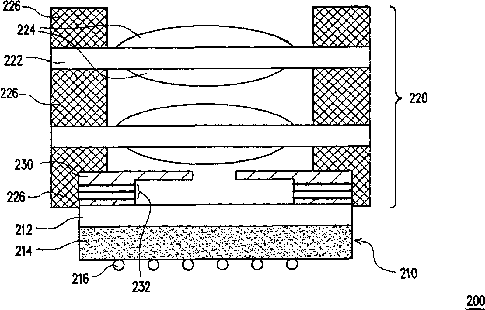
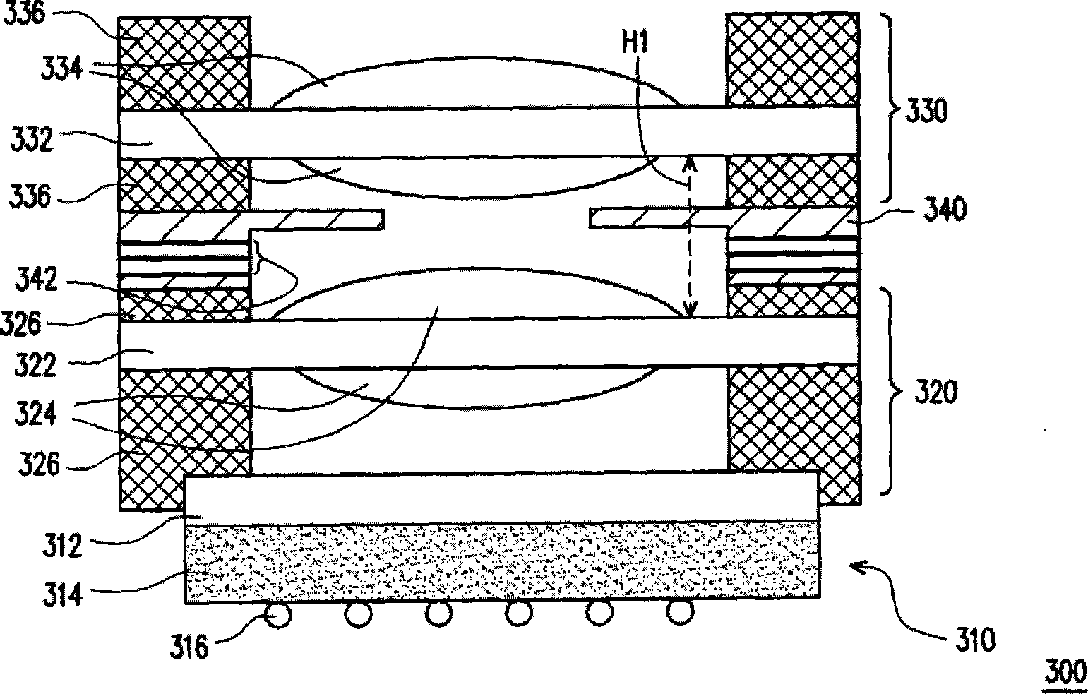
[0046] figure 2 It is a schematic diagram of an optical zoom system according to an embodiment of the present invention. Please refer to figure 2 , the optical zoom system 200 of this embodiment includes a light sensor 210 , a wafer-level optical lens module 220 and a focus motor 230 . In this embodiment, the light sensor 210 may be a complementary metal oxide semiconductor (CMOS) sensor or a charge coupled device (charge coupled devices, CCDs), wherein the light sensor 210 may be It includes a cover glass 212 , a light sensing element substrate 214 and a plurality of solder balls 216 . The cover glass 212 covers the light-sensing element substrate 214 , and the solder balls 216 are electrically connected to the light-sensing element substrate 214 .

[0047] The wafer-level optical lens module 220 is located on the light sensor 210, and the wafer-level optical lens module 220 includes at least one transparent substrate 222 and at least one lens 224, wherein at least one l...


PUM


Abstract

The invention discloses an optical zoom system, comprising an optical sensor, a wafer-degree optical lens module and a focusing motor, wherein the wafer-degree optical lens module is positioned on the optical sensor; the wafer-degree optical lens module comprises at least a transmitting substrate and at least a lens, wherein the lens is arranged on the transmitting substrate; and the focusing motor is positioned between the wafer-degree optical lens module and the optical sensor and is used for moving the wafer-degree optical lens module to enable the wafer-degree optical lens module to be far away or close to the optical sensor.

Description

technical field [0001] The present invention relates to an optical system, and in particular to an optical zoom system. Background technique [0002] With the trend of miniaturization and low-cost modules of electronic products, the emergence of Wafer Level Module (WLM) technology has attracted much attention. The wafer-level module technology mainly enables electronic products to utilize wafer-level manufacturing technology, thereby miniaturizing the volume of electronic products and reducing costs. Among them, the chip-level module technology can also be applied to the production of optical zoom systems, so that the volume of the optical zoom system can be much reduced compared with traditional optical zoom systems, and then can be applied to camera modules such as mobile phones. [0003] figure 1 It is a schematic diagram of an existing optical zoom system. Please refer to figure 1 , the optical zoom system 100 includes a light sensor 110 , an optical lens 120 and a f...

Claims


Application Information

Patent Timeline
Patent Type & Authority Patents(China)
IPC IPC(8): G02B7/04
Inventor 陈振亨
Owner HIMAX TECH LTD
Learn More