Lens component for electronic sensor optical imaging device and location method thereof

An electronic sensor and optical imaging technology, which is applied to color TV parts, TV system parts, electrical components, etc., can solve the problems of complex production process, high cost, unfavorable miniaturization, etc., and achieve low material cost and low production cost. Low cost and the effect of preventing adverse phenomena

Inactive Publication Date: 2011-07-20
李东
View PDF3 Cites 6 Cited by
  • Summary
  • Abstract
  • Description
  • Claims
  • Application Information

AI Technical Summary

Problems solved by technology

[0003] In order to solve the problems of high cost, unfavorable miniaturization and complex production process of the lens assembly of the electronic sensor opt

Method used


Image

  • Lens component for electronic sensor optical imaging device and location method thereof
  • Lens component for electronic sensor optical imaging device and location method thereof
  • Lens component for electronic sensor optical imaging device and location method thereof

Examples


Embodiment 1

[0033] Embodiment 3: The difference between this embodiment and Embodiment 1 is that the missing parts are two rectangles or two triangles or two fan-shaped or two irregular figures, and the two missing parts are arranged on two opposite sides. top corner or opposite sides.

Embodiment 2

[0034] Embodiment 4: The difference between this embodiment and Embodiment 1 is that the missing parts are three rectangles or three triangles or three fan shapes or three irregular figures.

Embodiment 3

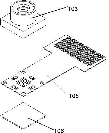
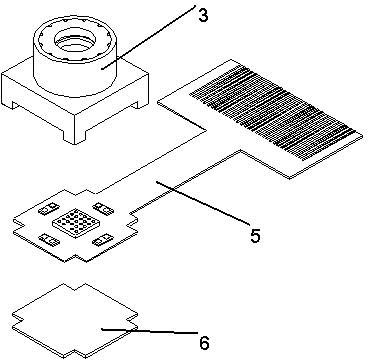
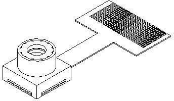
[0035] Embodiment 5: as Figure 6 to Figure 9 , a lens assembly of an electronic sensor optical imaging device, including a base 3, a sensor, and an FPC5 connected in sequence, and also includes a soft board reinforcement board 6, and the soft board reinforcement board 6 is fixedly arranged on the side of the FPC5 that is not connected to the sensor On the one hand, a raised portion is provided on the edge of the base 3 , and the raised portion is tightly connected with the periphery of the FPC 5 and the soft board reinforcing plate 6 .


PUM


Abstract

The invention provides a lens component for an electronic sensor optical imaging device and a location method thereof. The device comprises the lens component, a sensor, a flexible printing circuit (FPC) connected in sequence, and also comprises a soft board reinforcement plate; the soft board reinforcement plate is fixedly arranged on one side of the FPC not connected with the sensor; the bottom of the lens component is provided with a protrusion part; and an edge of the FPC and the soft board reinforcement plate is provided with a missing part in close fit connection with the protrusion part of a pedestal. A manufacturing method comprises the following steps of: bonding and fixing the soft board reinforcement plate and the FPC together, and arranging the missing part on the edge of the soft board reinforcement plate and the FPC; and arranging the protrusion part on the pedestal, wherein the protrusion part is in close fit connection with the missing part. In the invention, by the close fit connection of the protrusion part of the pedestal and the missing part on the edge of the FPC and the soft board reinforcement plate, the miniaturization production of a product is facilitated.

Description

technical field [0001] The present invention relates to a manufacturing method and device for an electronic sensor optical imaging system, in particular to a lens assembly of an electronic sensor optical imaging device and a manufacturing method thereof. Background technique [0002] like figure 1 As shown, the existing FPC-connected electronic sensor optical imaging system includes the following components connected in sequence: lens base 103 , sensor (not shown in the figure), FPC 105 , and reinforcing steel plate 106 . Description: FPC: flexible circuit board (flexible PCB): referred to as "soft board", also known as "flexible circuit board", also known as "flexible circuit board, flexible circuit board" or "flexible circuit board, flexible circuit board ". FPC is very soft, and the existing operation and production method is to use reinforcing steel plate to reinforce, FPC and reinforcing steel plate are bonded with glue, the specific process is as follows: ① Manually ...

Claims


Application Information

Patent Timeline
IPC IPC(8): H04N5/225
Inventor 李东
Owner 李东
Why Eureka
Try Eureka