Supercharge Your Innovation With Domain-Expert AI Agents!

Signal processing circuit and method thereof

A signal processing circuit and circuit technology, applied in electrical components, baseband system components, demodulation, etc., can solve the problems of insufficient automatic gain adjustment, spending a lot of time, and the receiver cannot distinguish the source of the signal, saving time. , the effect of reducing production costs

Inactive Publication Date: 2013-12-18
MSTAR SOFTWARE R&D (SHENZHEN) LTD +1
View PDF2 Cites 0 Cited by
  • Summary
  • Abstract
  • Description
  • Claims
  • Application Information

AI Technical Summary

Problems solved by technology

However, when a signal with high energy is encountered, since the automatic gain control circuit 160 is preset to set the gain to the maximum, the received signal will appear saturated. Once the signal is saturated, the receiving end cannot distinguish the source of the signal, so The automatic gain control circuit 160 needs to slowly reduce the gain until it is not saturated before performing signal detection. This step will take a lot of time. If the signal is too large, the original timing t 1 to t 7 The signal analysis time will not be enough for automatic gain adjustment and signal detection, which will affect the estimation of the carrier frequency offset by the carrier frequency offset compensation circuit 184

Method used


Image

  • Signal processing circuit and method thereof
  • Signal processing circuit and method thereof
  • Signal processing circuit and method thereof

Examples


Embodiment Construction

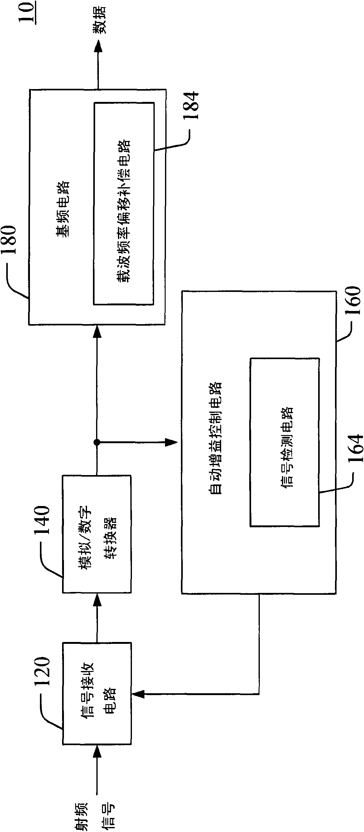
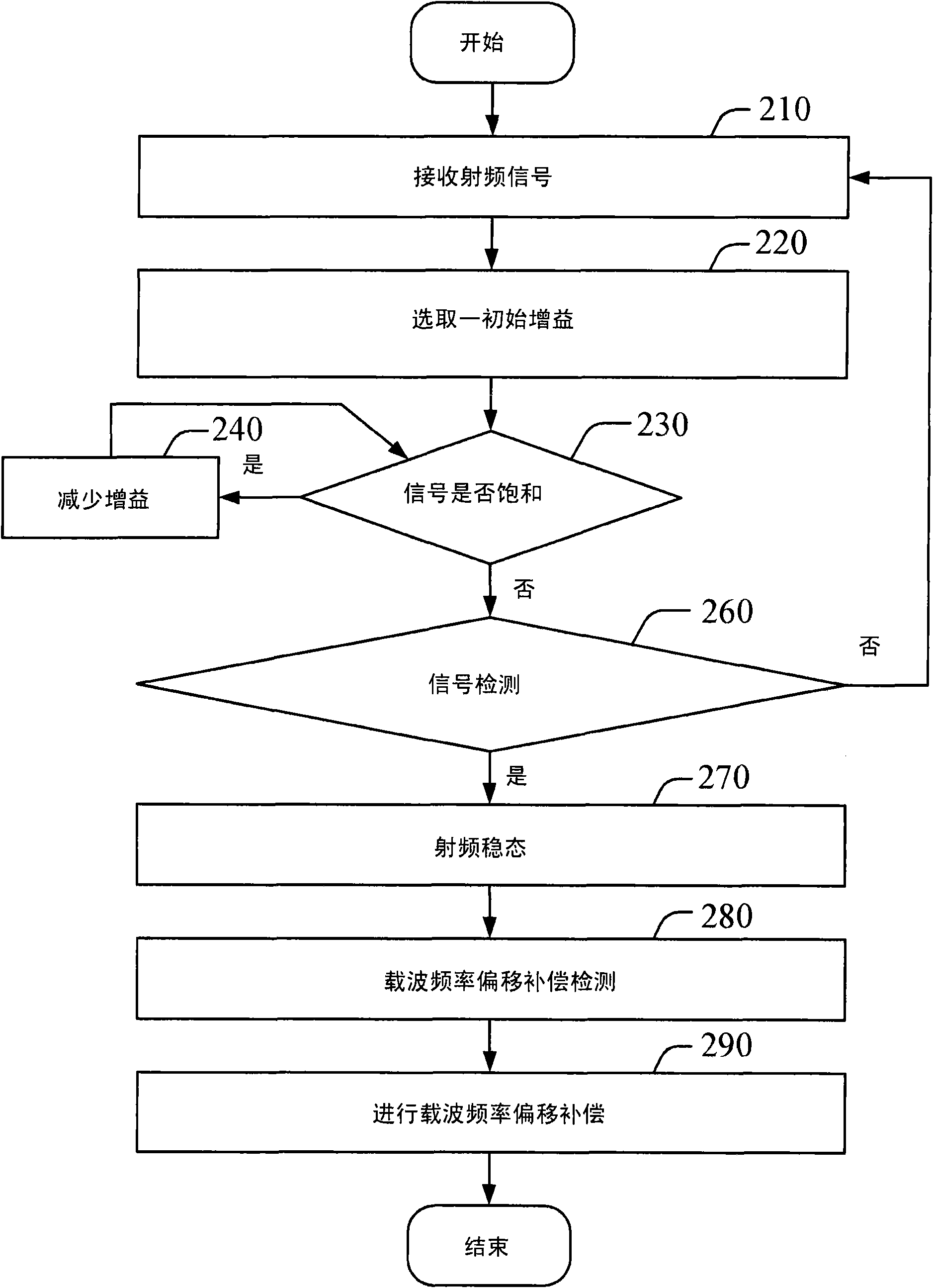
[0022] Figure 4 It is a functional block diagram of the signal processing circuit 40 of the present invention, including: a signal receiving circuit 420 , an analog / digital converter 440 , a signal analysis circuit 460 and a baseband circuit 480 . Figure 5 Please refer to the flow chart of the corresponding signal processing method.

[0023] In step 520, the signal receiving circuit 420 receives a radio frequency signal, adjusts the radio frequency signal according to the gain value generated by the signal analysis circuit 460, and converts the radio frequency signal into an analog signal. Then the analog signal is converted into a digital signal r(t) by the analog / digital converter 440, and the signal analysis circuit 460 generates a gain value to adjust the radio frequency signal according to the digital signal r(t); further, if the digital signal r(t) Unanalyzable means that the received signal is still in a saturated state. At this time, the signal analysis circuit 460 ...


PUM


Abstract

The invention discloses a signal processing circuit and method. The signal processing circuit comprises a signal receiving circuit, an analogue / digital (A / D) converter, a signal analysis circuit and a base frequency circuit, wherein the signal receiving circuit is used for receiving a radio frequency (RF) signal, adjusting the RF signal according to a gain value, and converting the RF signal into an analogue signal; the analogue / digital (A / D) converter is coupled to the signal receiving circuit and used for converting the analogue signal into a digital signal; the signal analysis circuit is coupled to the A / D converter and the signal receiving circuit and used for producing the gain value and a reference value according to the digital signal; and the base frequency circuit is coupled to the A / D converter and the signal analysis circuit and used for performing a carrier frequency offset compensation on the digital signal according to the reference value.

Description

technical field [0001] The present invention relates to a signal processing circuit and its method, in particular to a carrier frequency offset compensation circuit of the signal processing circuit and its method. Background technique [0002] In wireless transmission, due to the different distances between the transmitting end and the receiving end, the receiving end may receive signals with different energy levels. Therefore, it is necessary to adjust the gain of the receiving end through an automatic gain control circuit (auto-gain control, AGC) to make it Signals with different energy levels can be correctly received. [0003] figure 1 It is a functional block diagram of the existing signal processing circuit 10 , including: a signal receiving circuit 120 , an analog-to-digital converter (analog-to-digital converter, ADC) 140 , an automatic gain control circuit 160 and a baseband circuit 180 . Automatic gain control circuit 160 includes signal detection circuit 164 . ...

Claims


Application Information

Patent Timeline
Patent Type & Authority Patents(China)
IPC IPC(8): H03D7/00H04L25/02
Inventor 庄景翔何天行洪绍评童泰来
Owner MSTAR SOFTWARE R&D (SHENZHEN) LTD
Features
  • R&D
  • Intellectual Property
  • Life Sciences
  • Materials
  • Tech Scout
  • Unparalleled Data Quality
  • Higher Quality Content
  • 60% Fewer Hallucinations
Learn More