System and method for designing integrated circuits that employ adaptive voltage scaling optimization

An integrated circuit, a technique for designing circuits, applied in the field of integrated circuit design, capable of solving problems such as obstruction, setup or hold time violation, and damage to circuit logic

Active Publication Date: 2014-05-07
AVAGO TECH WIRELESS IP SINGAPORE PTE
View PDF3 Cites 0 Cited by
  • Summary
  • Abstract
  • Description
  • Claims
  • Application Information

AI Technical Summary

Problems solved by technology

A setup or hold time violation breaks the logic of the circuit and prevents it from doing what it was designed to do

Method used


Image

  • System and method for designing integrated circuits that employ adaptive voltage scaling optimization
  • System and method for designing integrated circuits that employ adaptive voltage scaling optimization
  • System and method for designing integrated circuits that employ adaptive voltage scaling optimization

Examples


Embodiment Construction

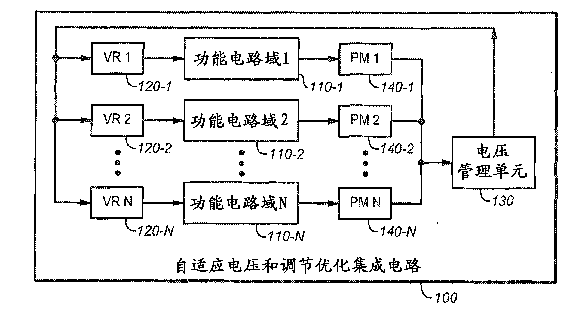
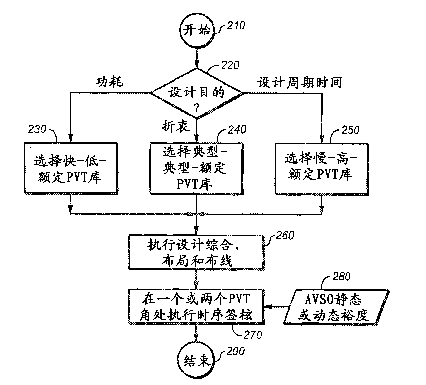
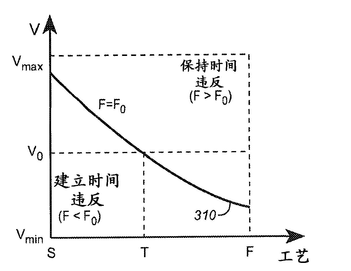
[0020] It has been found that conventional IC design flows fail to take advantage of the AVSO IC's ability to adjust its supply voltage in real time to achieve signal propagation speed adjustment. A better design flow for AVSO ICs would allow the circuit designer to predetermine whether power consumption, rapid development (also known as turnaround) time, or a tradeoff between the two is the design goal. It has also been found that implementing the slow and fast PVT and RC corner results of conventional signoff timing is inappropriate for AVSO ICs. The timing signoff of the AVSO IC should advantageously utilize values ​​of PVT and RC corners and on OCV margins that are never considered by the conventional timing signoff process.

[0021] Various embodiments of systems and methods for designing AVSO ICs are described herein. The main purpose when designing any IC is to generate the F 0 The following design works as expected. Various embodiments described herein allow circuit...


PUM


Abstract

A design process optimization system and method for designing a circuit, which may be an integrated circuit (IC) employing adaptive voltage and scaling optimization (AVSO). In one embodiment, the system includes: (1) a process-voltage-temperature (PVT) libraries database configured to contain PVT libraries of PVT characterizations of devices of cells from which the circuit is to be constructed and (2) a PVT library selector coupled to the PVT libraries database and configured to receive a selection indicating a supplemental objective and respond to the selection by selecting one of the PVT libraries from the PVT libraries database, a timing signoff tool later employing at most two corners from the one of the PVT libraries to perform a timing signoff with respect to the circuit.

Description

[0001] Cross Reference to Provisional Application [0002] This application is related to U.S. Provisional Application Serial No. 61 / 126,881, entitled "A Novel Paradigm for Optimizing Performance, Power, Area and / or Yield in Integrated Circuits," filed May 7, 2008 by Parker et al. The invention is commonly assigned and is incorporated herein by reference. technical field [0003] The present invention relates generally to integrated circuit (IC) design, and more particularly, to systems and methods for designing ICs using Adaptive Voltage and Regulation Optimization (AVSO). Background technique [0004] Circuit designers use electronic design automation (EDA) tools, a class of computer-aided design (CAD) tools, to design and lay out electronic circuits, including simulating circuit operation, determining the logic of cells (i.e., devices including, for example, transistors) components) should be placed and where the interconnects coupling the cells together should be routed...

Claims


Application Information

Patent Timeline
Patent Type & Authority Patents(China)
IPC IPC(8): G06F17/50
CPCG06F17/505G06F30/327
Inventor A·泰特巴姆
Owner AVAGO TECH WIRELESS IP SINGAPORE PTE
Why Eureka
Try Eureka