

LED adhesive luminescent panel
A light-emitting board and lamination technology, applied in the direction of semiconductor devices, light sources, electric light sources, etc. of light-emitting elements, can solve the problems of inconvenience and time-consuming to do these things
- Summary
- Abstract
- Description
- Claims
- Application Information
AI Technical Summary
Problems solved by technology
Method used
Image

Examples
Embodiment Construction
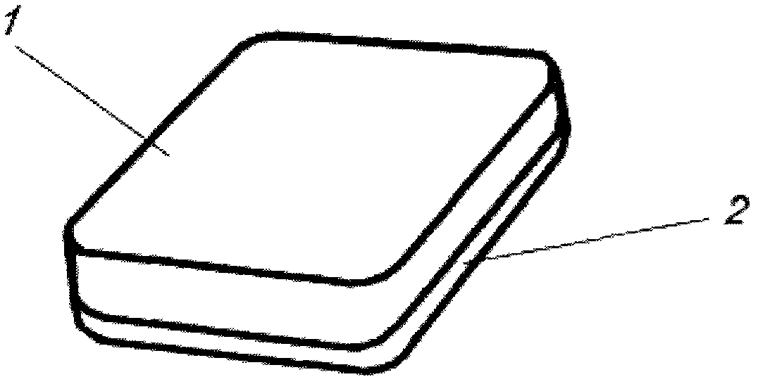
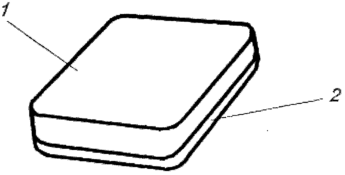
[0015] now attached figure 1 The present invention will be further described.
[0016] Such as figure 1 As shown, an LED bonding luminescent board is characterized in that: the front surface of the LED bonding luminescent board is a push switch 1 made of a transparent material or a translucent material, and the push switch 1 is also formed as a lampshade. The interior of the LED bonding light-emitting board is an LED light-emitting lamp and a battery (not shown in the internal structure diagram) that supplies power to the LED light-emitting lamp. The rear surface of the LED bonding light-emitting board can be bonded and fixed to other objects. There are 2 fitting and fixing devices on the top, and the fitting and fixing device 2 is a suction cup device or a magnetic adsorption device.
PUM
 Abstract
Description
Claims
Application Information