
Manufacturing process of soft-type printed circuit board with different appearances at upper and lower layers

A printed circuit board and manufacturing process technology, applied in the direction of multi-layer circuit manufacturing, can solve problems such as inability to manufacture, achieve the effects of reducing assembly space, avoiding damage to the appearance, and reducing costs

Active Publication Date: 2011-09-14
CHUNHUA TECHNOLOGICAL KUSN
View PDF7 Cites 0 Cited by
  • Summary
  • Abstract
  • Description
  • Claims
  • Application Information

AI Technical Summary

Problems solved by technology

Mechanisms with different shapes cannot be manufactured because the common area between the two layers cannot be directly drilled with steel molds and interfere with each other.

Method used


Image

  • Manufacturing process of soft-type printed circuit board with different appearances at upper and lower layers
  • Manufacturing process of soft-type printed circuit board with different appearances at upper and lower layers
  • Manufacturing process of soft-type printed circuit board with different appearances at upper and lower layers

Examples


Embodiment 1

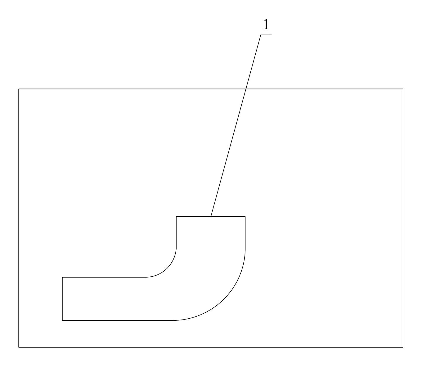
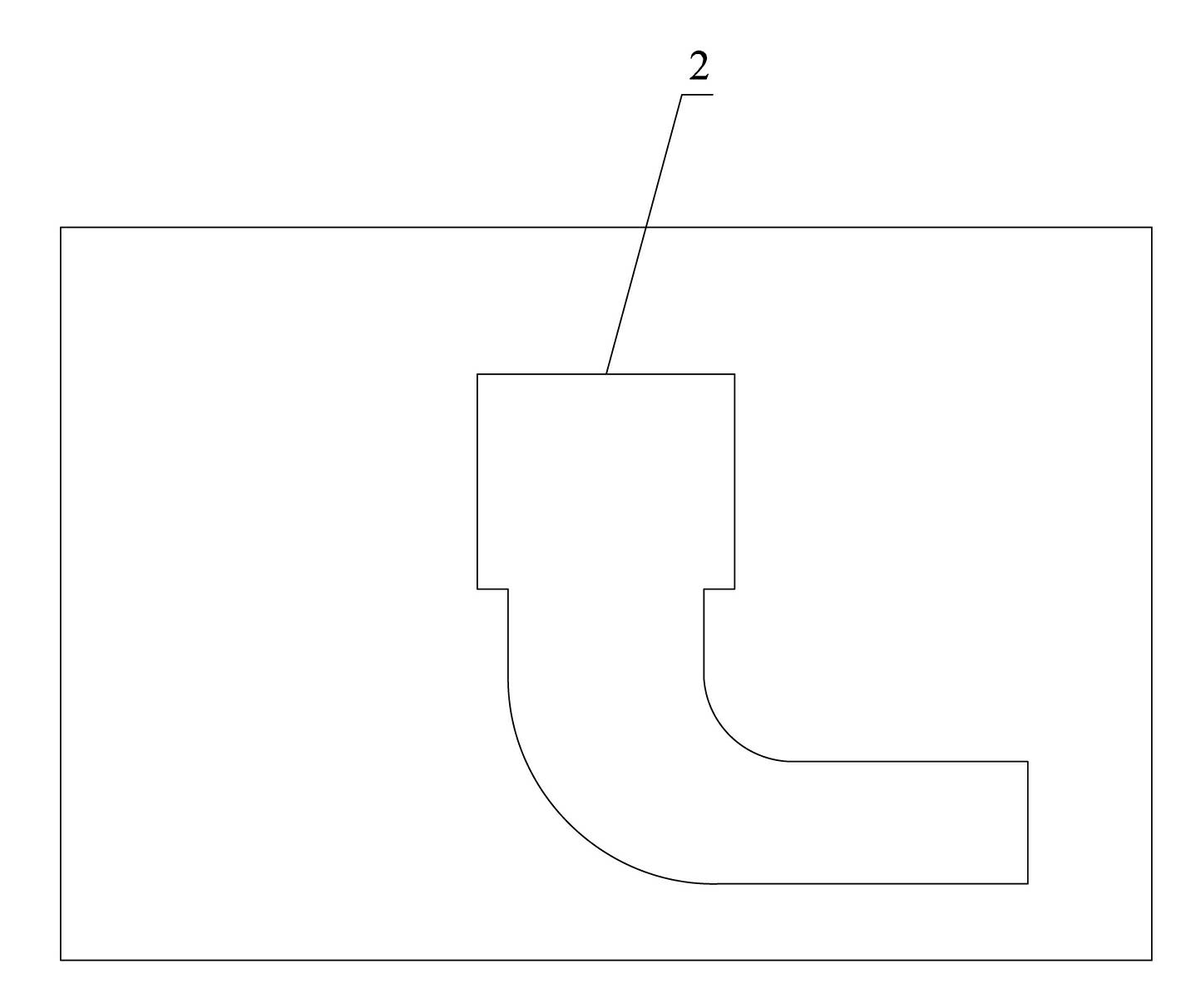
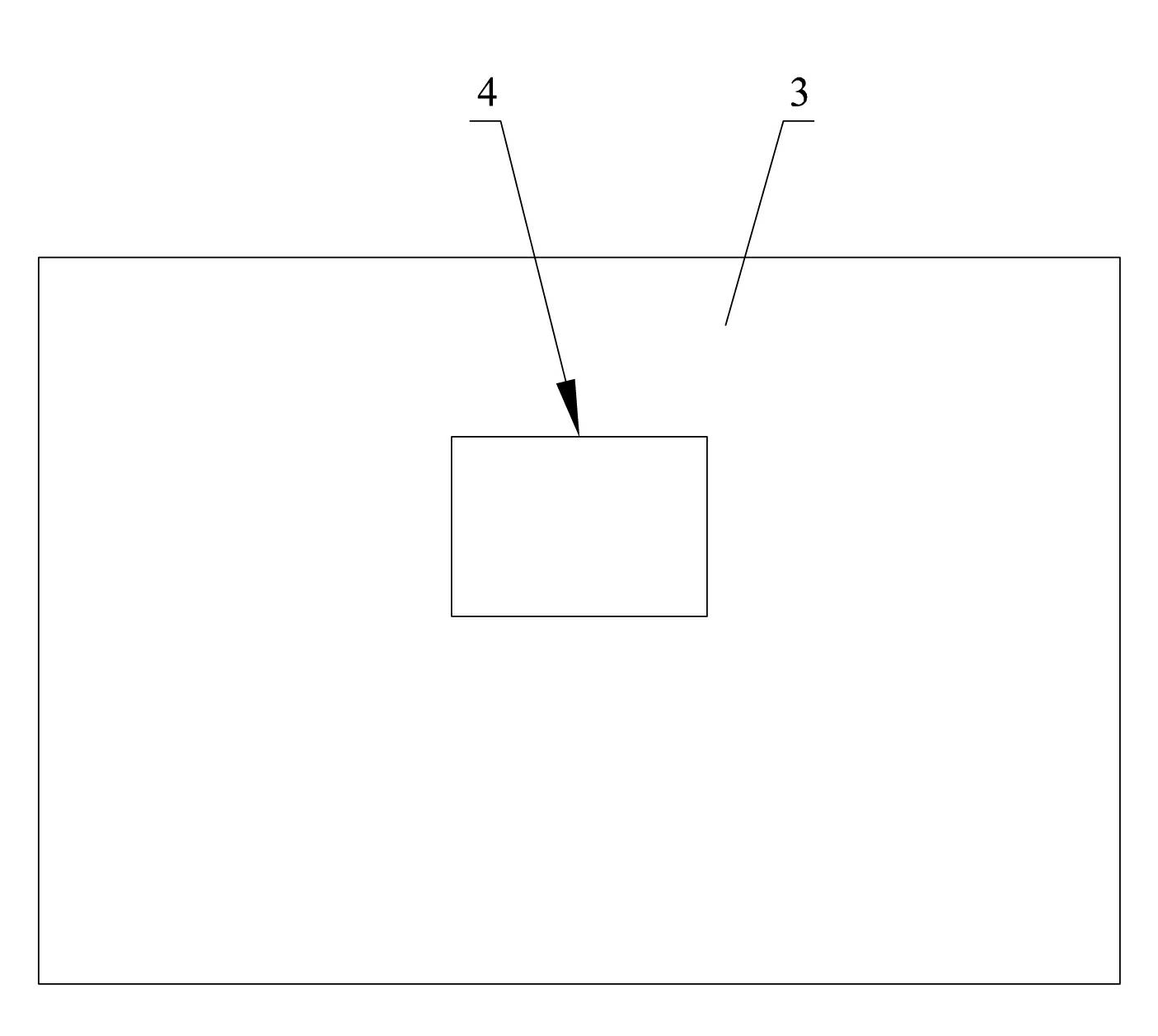
[0023] Embodiment one: see attached figure 1 to attach Figure 5 shown.

[0024] A manufacturing process of flexible printed circuit boards with different shapes on the upper and lower layers, which is used to make the first stack 1 and the second stack 2 of the flexible printed circuit boards with different shapes on the upper and lower layers, which includes the following steps:

[0025] (1) An auxiliary layer 3 made of PI is added between the first stack 1 and the second stack 2; in the same shape area of ​​the first stack 1 and the second stack 2, the auxiliary layer has a hollow avoidance zone 4;

[0026] (2) After the above-mentioned first stack 1 and second stack 2 with the auxiliary layer 3 are produced according to the general process, pull out the 5 holes in the edge area of ​​the same shape area of ​​the first stack 1 and the second stack 2 ;

[0027] (3) Die-cut the first stack 1 and the second stack 2 according to their shapes by half-cutting or laser method; ...


PUM


Abstract

The invention relates to a manufacturing process of a soft printed circuit board with different appearances at upper and lower layers, which is used for manufacturing a first stack and a second stack of the soft printed circuit board with different appearances at upper and lower layers. The manufacturing process comprises the following steps of: (1) adding an auxiliary layer between the first stack and the second stack, wherein the auxiliary layer is provided with hollow dodging areas in identical-appearance areas of the first stack and the second stack; (2) after the first stack and the second stack having duplicate layers are manufactured based on a general flow, unfolding edge area cavities of the identical-appearance areas of the first stack and the second stack; (3) die cutting the first stack and the second stack according to the appearances of the first stack and the second stack respectively; and (4) drawing out the auxiliary layer to obtain the soft printed circuit board withdifferent appearances at upper and lower layers. Since the auxiliary layer is added between the stacks with different appearances in the invention, appearance damage caused by mutual interference of the appearances is avoided, and soft circuit boards with different appearances are integrated together to reduce the cost and assembly space of adapting parts.

Description

technical field [0001] The invention relates to a manufacturing process of a flexible printed circuit board with different shapes on the upper and lower layers, and belongs to the technical field of flexible circuit board production. Background technique [0002] Generally, the appearance design of the stacked structure of the flexible printed circuit board is generally the same appearance, which is produced by direct hole extraction of the mold. Products with different shapes need to use two flexible boards to transfer through the connector. Mechanisms with different shapes cannot be manufactured because the common area between the two layers cannot be directly drilled with steel molds and interferes with each other. Contents of the invention [0003] The object of the present invention is to provide a manufacturing process of flexible printed circuit boards with different shapes on the upper and lower layers, which avoids mutual interference between stacked structures o...

Claims


Application Information

Patent Timeline
Patent Type & Authority Applications(China)
IPC IPC(8): H05K3/46
Inventor 顾大余莫卫龚
Owner CHUNHUA TECHNOLOGICAL KUSN
Learn More