Eureka AIR delivers breakthrough ideas for toughest innovation challenges, trusted by R&D personnel around the world.

Nanoscale electrode processing method based on AFM (atomic force microscopy)

A technology of electrode processing and nano-electrode, which is applied in the manufacture of circuits, electrical components, semiconductors/solid-state devices, etc. It can solve problems such as difficulty in obtaining cutting-edge electrodes, no record of nano-scale electrodes, and difficulty in meeting detection requirements for electrodes, so as to achieve easy operation Sexuality and low cost effect

Inactive Publication Date: 2014-02-12
SHENYANG INST OF AUTOMATION - CHINESE ACAD OF SCI
View PDF6 Cites 0 Cited by
  • Summary
  • Abstract
  • Description
  • Claims
  • Application Information

AI Technical Summary

Problems solved by technology

[0003] In order to carry out nanofluidic research, especially single-molecule detection (DNA rapid sequencing), it is difficult to meet the detection requirements for electrodes with a width on the order of microns. How to process nanoscale electrodes for higher sensitivity detection has become the primary problem to be solved.
The current chip manufacturing technology usually adopts MEMS (short for Micro Electro Mechanical System) process, and it is difficult to obtain electrodes within 100 nanometers of the tip through vapor deposition.
Currently, methods for fabricating nanoscale electrodes using AFM have not been documented

Method used


Image

  • Nanoscale electrode processing method based on AFM (atomic force microscopy)
  • Nanoscale electrode processing method based on AFM (atomic force microscopy)
  • Nanoscale electrode processing method based on AFM (atomic force microscopy)

Examples


Embodiment Construction

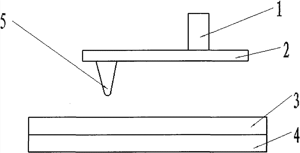
[0021] The working status of the present invention is as figure 1 As shown, 1 is PZT, 2 is AFM cantilever beam, 3 is gold electrode, 4 is silicon dioxide, and 5 is probe.

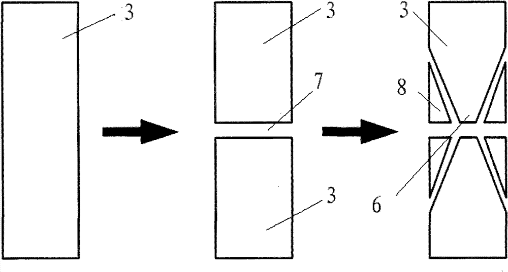
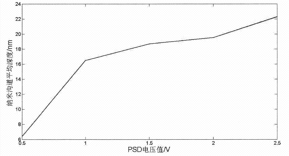
[0022] 1) Determine the relationship between cutting depth and PSD signal: as figure 1 , figure 2 As shown, the probe 5 processes a nano-channel 7 on the substrate, and at the same time divides the gold electrode 3 into a pair. In order to determine the cutting depth, it is first necessary to determine the relationship between the cutting depth and the PSD signal: for a silicon dioxide substrate in several Nano-channels with a certain depth are processed under different PSD voltage values ​​(from small to large), and the processed nano-channels are scanned and imaged, and the depth values ​​corresponding to different PSD signals are measured, and the fitting results are as follows: image 3 The graph of the relationship between voltage and depth is shown;

[0023] 2) Processing of nanochannels: Assuming...


PUM


Abstract

The invention discloses a nanoscale electrode processing method based on an AFM (atomic force microscopy). According to the method, a micrometer level electrode is cut and processed through the controlling on the action force of an AFM probe on a sample and the movement path and speed of the probe, thus the processing of the nanoscale electrode of which a front end has width within100 nanometers is realized, and the detection accuracy and flexibility in a nano fluidic test are increased. The nanoscale electrode processing method provided by the invention can be applied to high-flexibility detection and analysis of the fluid characteristics of fluid in a nano channel in the nano fluidic chip and biology monomolecules.

Description

technical field [0001] The invention relates to the technical field of nano-processing, in particular to an AFM-based nano-scale electrode processing method. Background technique [0002] In recent years, the research and application of microfluidic chip technology in the fields of disease diagnosis, drug screening, and environmental detection has become increasingly widespread. etc. played an important role. With the development of technology, biomedical research and applications have begun to be carried out at the molecular, DNA, and protein levels. Microfluidic technology has been difficult to meet the needs of smaller-scale, smaller-dose, and higher-sensitivity detection and analysis of samples at the molecular level. Therefore, the smaller-scale chip technology-"nanofluidic control" has become a new focus of attention. [0003] In order to carry out nanofluidic research, especially single-molecule detection (DNA rapid sequencing), it is difficult for electrodes with a...

Claims


Application Information

Patent Timeline
Patent Type & Authority Patents(China)
IPC IPC(8): H01L21/44
Inventor 焦念东王志迁董再励
Owner SHENYANG INST OF AUTOMATION - CHINESE ACAD OF SCI
Why Eureka
Eureka Blog
Learn More