

AFM (Atomic Force Microscopy)-based processing method of nanometer channel
A processed and substrate technology, applied in the direction of nanotechnology, nanotechnology, nanostructure manufacturing, etc., to achieve the effect of low cost and easy operation
- Summary
- Abstract
- Description
- Claims
- Application Information
AI Technical Summary
Problems solved by technology
Method used
Image

Examples
Embodiment
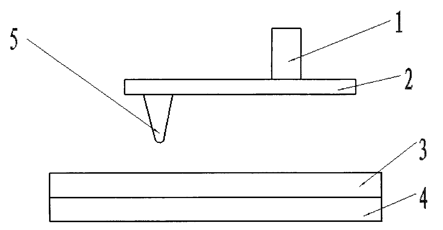
[0034] 1) Calibration of the sensitivity (PSD sensitivity) of the photoelectric position detection sensor and determination of the elastic modulus of the processed material (silicon dioxide):
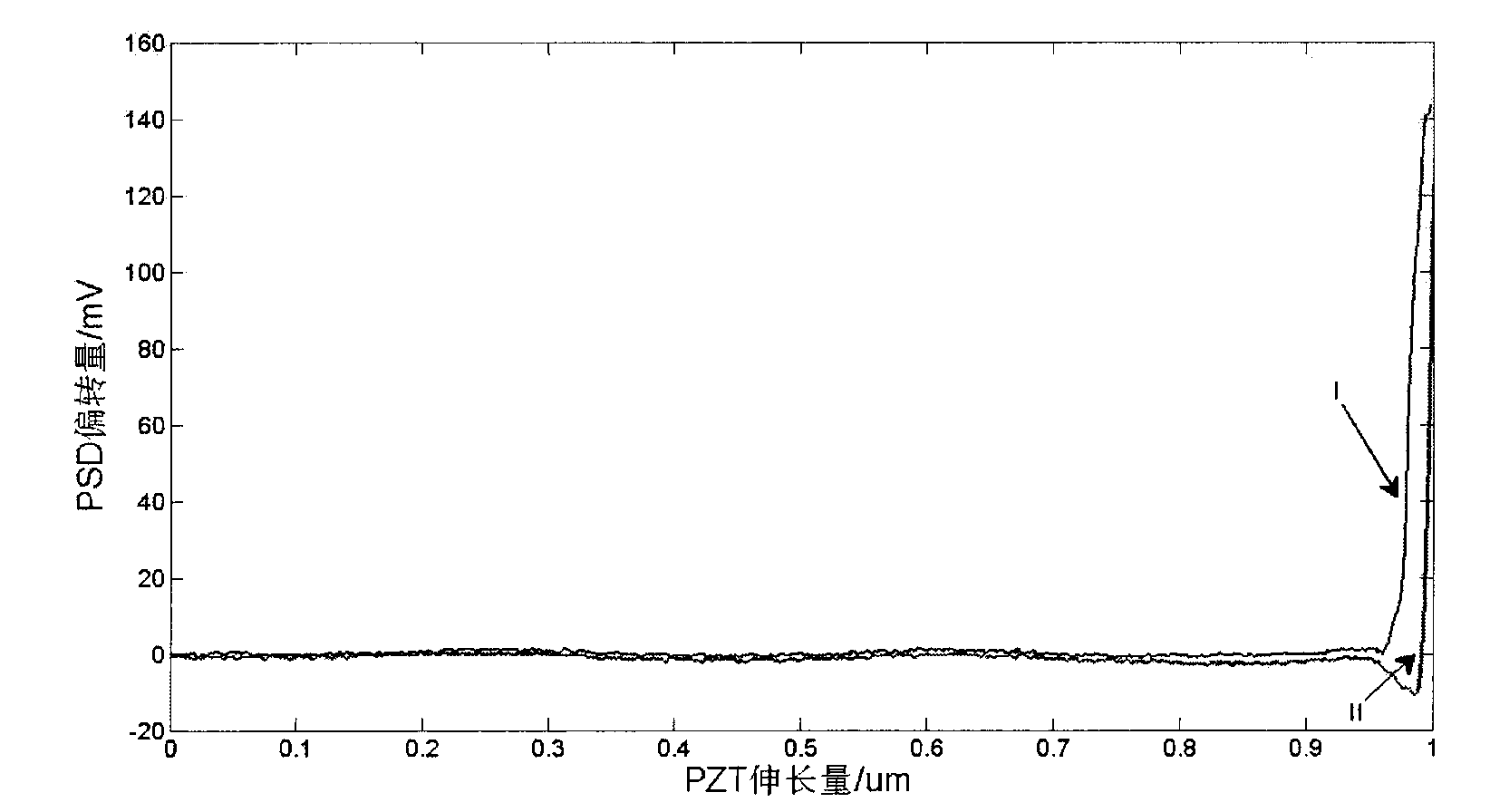
[0035] Do force curves on silica substrates, such as figure 2 As shown, the abscissa is the vertical elongation of PZT, and the ordinate is the vertical deflection of PSD. From this curve, use the nanoscope software of American Veeco Company to calibrate the PSD sensitivity, s=56.13nm / V; use the Herz model: F is the elastic recovery force of the cantilever beam, k=40N / m, R=25nm, s×v is 4.39nm, δ is 6nm, and then according to E. tip Assumed to be infinite, ν substrate is 0.12, calculate E * =1.79GPa, the modulus of elasticity E of the processed material substrate 1.77Gpa;
[0036] 2) Determination of the distance from the probe to the substrate: gradually increase the elongation of the PZT in the vertical direction, each time a fixed increase of 5nm and record the number of incre...
PUM
 Abstract
Description
Claims
Application Information