Semiconductor laser device and display device
A technology of laser devices and semiconductors, which is applied in semiconductor laser devices, semiconductor lasers, laser devices, etc., and can solve problems such as large output
- Summary
- Abstract
- Description
- Claims
- Application Information
AI Technical Summary
Problems solved by technology
Method used
Image

Examples
no. 1 approach
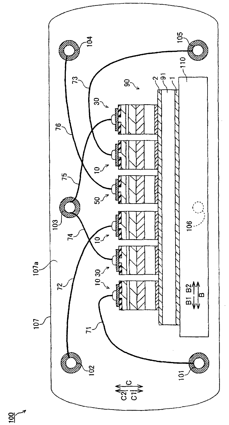
[0063] First, refer to figure 1 with figure 2 The structure of the semiconductor laser device 100 according to the first embodiment of the present invention will be described.
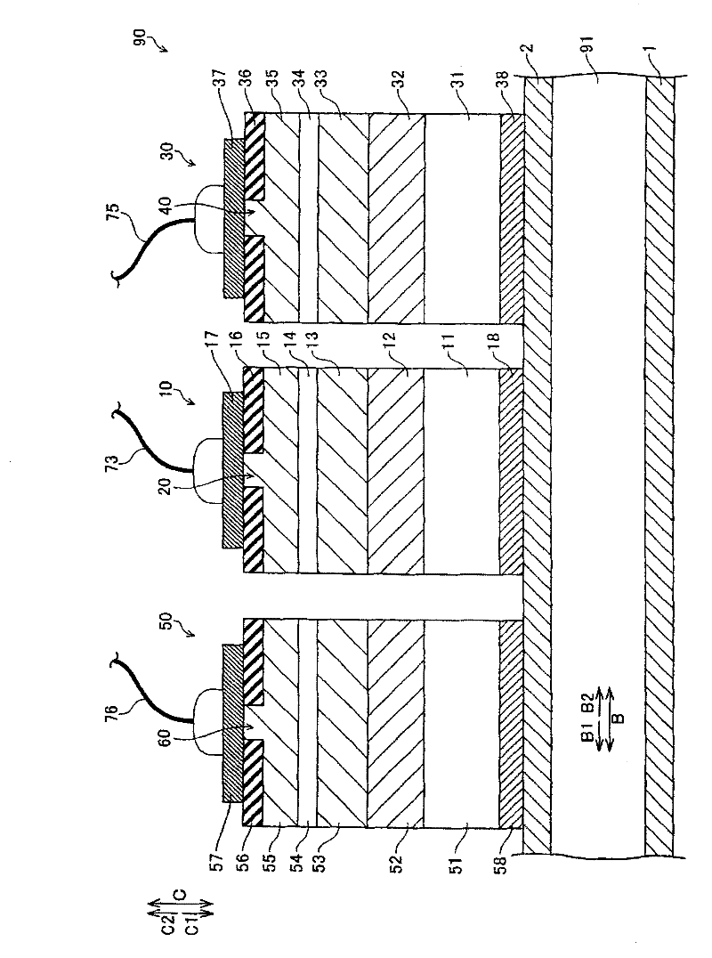
[0064] Such as figure 1 As shown, in the semiconductor laser device 100 according to the first embodiment of the present invention, the RGB three-wavelength semiconductor laser element unit 90 is fixed to the upper surface (surface on the C2 side) of the pedestal 110 via a conductive adhesive layer 1 such as AuSn solder. In addition, in the RGB three-wavelength semiconductor laser element part 90, there is a red semiconductor laser element 10 with an oscillation wavelength of about 655 nm, a green semiconductor laser element 30 with an oscillation wavelength of about 530 nm, and a blue semiconductor laser element 50 with a wavelength of about 480 nm. The laser beams of each color are fixed to the upper surface of the base 91 at predetermined intervals through a conductive adhesive layer 2 such as Au...
no. 2 approach
[0107] refer to Figure 6 ~ Figure 8 A second embodiment will be described. In this second embodiment, different from the above-mentioned first embodiment, a monolithic red semiconductor laser element unit 210 integrating four red semiconductor laser elements 210a to 210d is arranged on a submount 291, and two green semiconductor laser elements 210a to 210d are integrated. A case where the monolithic green semiconductor laser element unit 230 and one blue semiconductor laser element 50 in which the semiconductor laser elements 230a and 230b are integrated constitutes the RGB three-wavelength semiconductor laser element unit 290 will be described.
[0108] Such as Image 6 As shown, in the semiconductor laser device 200 according to the second embodiment of the present invention, the RGB three-wavelength semiconductor laser element portion 290 is fixed to the upper surface (surface on the C2 side) of the pedestal 206 .
[0109] Here, if Figure 7 As shown, in the second embo...
no. 3 approach
[0119] refer to Image 6 with Figure 8 ~ Figure 12 A third embodiment will be described. In this third embodiment, unlike the above-mentioned second embodiment, the green semiconductor laser element unit 330 composed of two green semiconductor laser elements 330a and 330b and one blue semiconductor laser element 350 are arranged and integrated on a base 391. The case where the RGB three-wavelength semiconductor laser element portion 390 is configured by the monolithic two-wavelength semiconductor laser element portion 370 and the red semiconductor laser element portion 210 will be described.
[0120] Such as Figure 9 As shown, in the semiconductor laser device 300 according to the third embodiment of the present invention, the RGB three-wavelength semiconductor laser element unit 390 is fixed on the upper surface of the base 206 .
[0121] Here, if Figure 9 As shown, in the third embodiment, in the RGB three-wavelength semiconductor laser element part 390, the red semic...
PUM
| Property | Measurement | Unit |
|---|---|---|
| Thickness | aaaaa | aaaaa |
| Thickness | aaaaa | aaaaa |
| Thickness | aaaaa | aaaaa |
Abstract
Description
Claims
Application Information
 - R&D
- Intellectual Property
- Life Sciences
- Materials
- Tech Scout
- Unparalleled Data Quality
- Higher Quality Content
- 60% Fewer Hallucinations
Browse by: Latest US Patents, China's latest patents, Technical Efficacy Thesaurus, Application Domain, Technology Topic, Popular Technical Reports.
© 2025 PatSnap. All rights reserved.Legal|Privacy policy|Modern Slavery Act Transparency Statement|Sitemap|About US| Contact US: help@patsnap.com