

Method for realizing light transmission of thin film solar module by using vibrating mirror laser equipment
A solar thin film and laser equipment technology, applied in laser welding equipment, electrical components, welding equipment, etc., can solve the problems affecting the efficiency and yield of components, the inability to change graphics and patterns, and affecting the electrical characteristics of batteries, etc., to achieve high work efficiency , Graphic changes are flexible, and the effect is easy to achieve
- Summary
- Abstract
- Description
- Claims
- Application Information
AI Technical Summary
Problems solved by technology
Method used
Image

Examples
Embodiment 1
[0028] The method for realizing the light transmission of the solar thin film battery module by applying the galvanometer laser device includes the following steps:
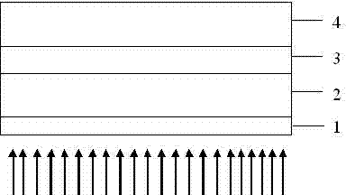
[0029] a. See attached figure 1 : On the float glass substrate 1, use low-pressure chemical vapor deposition technology or magnetron sputtering technology to deposit a transparent conductive film as the front electrode layer 2 of the battery; then use plasma chemical vapor deposition technology (PECVD) to coat the glass substrate Thin-film silicon p-i-n or p-i-n / p-i-n laminate structure and triple-junction silicon-based thin-film photoelectric conversion layer 3 are deposited on it; a transparent conductive film is grown on the above photoelectric conversion layer by low-pressure chemical vapor deposition technology as the back electrode layer 4 of the battery;
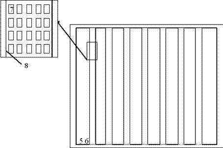
[0030] b. See attached figure 2 : the present embodiment adopts strip-shaped insulating area 5, and this area is used for carrying out light-transmitt...
Embodiment 2
[0038] The method for realizing the light transmission of the solar thin film battery module by applying the galvanometer laser device includes the following steps:
[0039] a. See attached figure 1 : On the float glass substrate 1, use low-pressure chemical vapor deposition technology or magnetron sputtering technology to deposit a transparent conductive film as the front electrode layer 2 of the battery; then use plasma chemical vapor deposition technology (PECVD) to coat the glass substrate Thin-film silicon p-i-n or p-i-n / p-i-n laminate structure and triple-junction silicon-based thin-film photoelectric conversion layer 3 are deposited on it; a transparent conductive film is grown on the above photoelectric conversion layer by low-pressure chemical vapor deposition technology as the back electrode layer 4 of the battery;
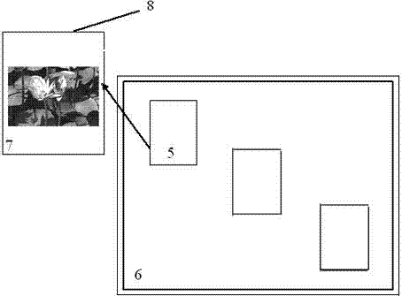
[0040] b. See attached image 3 : The present embodiment adopts a rectangular insulating area 5, which is used for light-transmitting treatment, and th...
PUM
| Property | Measurement | Unit |
|---|---|---|
| wavelength | aaaaa | aaaaa |
| transmittivity | aaaaa | aaaaa |
Abstract
Description
Claims
Application Information