Method and device for improving non-uniform thickness in blade-feeding position during multi-line cutting of silicon chip

A technology of multi-wire cutting and silicon wafers, which is applied in the direction of fine working devices, working accessories, stone processing equipment, etc., can solve the problems of uneven thickness of multi-wire cutting silicon wafers, and achieve the improvement of uneven thickness. The method is scientific and the selection convenient effect

Inactive Publication Date: 2011-11-16
浙江光益硅业科技有限公司
View PDF8 Cites 4 Cited by
  • Summary
  • Abstract
  • Description
  • Claims
  • Application Information

AI Technical Summary

Problems solved by technology

[0006] In order to solve the problem of uneven thickness of the existing multi-wire cutting silicon wafer, the present invention provides a met

Method used


Image

  • Method and device for improving non-uniform thickness in blade-feeding position during multi-line cutting of silicon chip
  • Method and device for improving non-uniform thickness in blade-feeding position during multi-line cutting of silicon chip
  • Method and device for improving non-uniform thickness in blade-feeding position during multi-line cutting of silicon chip

Examples


Embodiment Construction

[0018] The method and device of the present invention will be further described below in conjunction with examples of implementation.

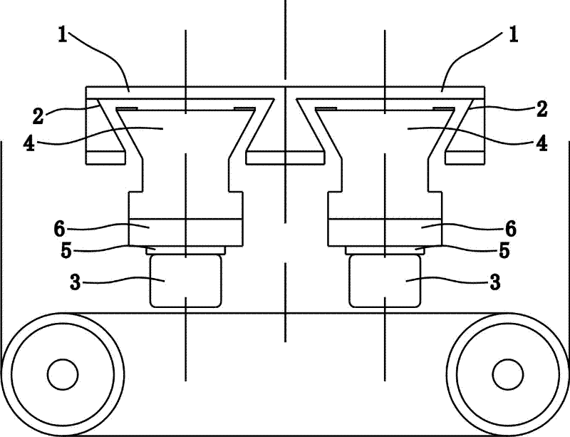
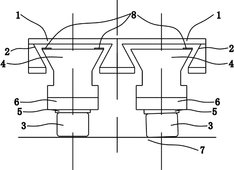
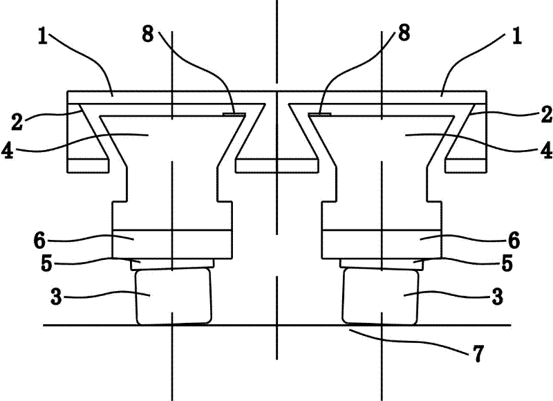
[0019] see Figure 1-5 , this embodiment includes a feeding mechanism 1, a dovetail groove 2 arranged on the feeding mechanism 1, a workpiece pressing block 4 for fixing a workpiece 3 (ie, a silicon rod or a silicon ingot), a workpiece 3 bonded by an adhesive, glass Bar 5, workpiece connecting plate 6, workpiece pressing block 4 is connected with workpiece connecting plate 6, several inserting pieces 8, wherein, one of several inserting pieces 8 or several stacking inserting pieces 8 are arranged on one end or two of workpiece pressing block 4 tops The end is located between the workpiece pressing block 4 and the dovetail groove 2 and the top wall of the dovetail groove 2, and the starting position of the workpiece 3 in the same group is adjusted to be consistent with the parallelism of the touch of the wire net 7.

[0020] The inserting shee...


PUM


Abstract

The invention discloses a method and device for improving the thickness uniformity in a blade-feeding position during the multi-line cutting of a silicon chip. The device comprises a feeding mechanism, a dovetail groove arranged on the feeding mechanism, a workpiece pressure block for fixing workpieces, the workpieces bonded by adhesives, a glass strip, a workpiece connecting plate and a plurality of insertion pieces, wherein the workpiece pressure block is connected with the workpiece connecting plate, one of the insertion pieces or multiple superimposed insertion pieces are arranged at one end or two ends at the top of the workpiece pressure block and positioned between the top end of the workpiece pressure block and the top wall of the dovetail groove, and the parallelism and the height difference between the feeding initial positions of the workpieces in the same group and a linear mesh contact surface are regulated to be consistent. By measuring and regulating the parallelism of the feeding initial positions of the workpieces and further utilizing the existing feeler gauges in complete specifications to precisely regulate the height difference between the feeding initial positions of the workpieces and the linear mesh contact surface, the invention achieves the purposes of enabling the parallelism between the feeding initial positions of the cut workpieces in the same group and the linear mesh contact surface to be consistent and effectively improving the non-uniform thickness in a blade-feeding position during the multi-line cutting of a silicon chip.

Description

technical field [0001] The invention relates to a thickness control technology for processing monocrystalline silicon wafers for semiconductors and monocrystalline / polycrystalline silicon wafers for solar cells in the field of multi-wire cutting, and in particular to a method and device for improving the uneven thickness at the edge of a multi-wire cutting silicon wafer. Background technique [0002] Silicon wafers are the main building blocks in the semiconductor and photovoltaic fields. Silicon wafer multi-wire cutting technology is a relatively advanced silicon wafer processing technology in the world at present. It is different from traditional cutting methods such as saw blades and grinding wheels, and is also different from laser cutting. It is driven by a high-speed moving steel wire. The cutting edge attached to the steel wire rubs against the silicon rod to achieve the purpose of cutting. During the whole process, the steel wire is guided by several wire pulleys t...

Claims


Application Information

Patent Timeline
IPC IPC(8): B28D5/04B28D7/00
Inventor 汪贵发蒋建松
Owner 浙江光益硅业科技有限公司
Why Eureka
Try Eureka